


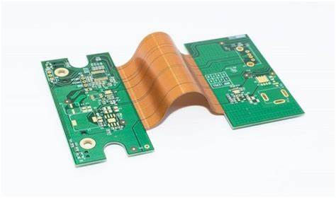
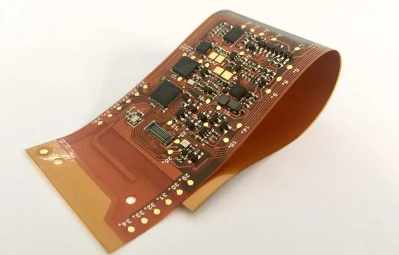
What is a Flex Harness PCB?
A flex harness PCB, also known as a flexible printed circuit board (FPCB) or flex circuit, is a type of printed circuit board that is made of a flexible polymer material like polyimide or polyester. Unlike traditional rigid PCBs, flex harnesses can bend and flex to accommodate different form factors and allow dynamic movement.
Flex harnesses consist of conductive tracks or traces etched or printed onto a thin flexible substrate. These traces interconnect different components mounted directly onto the flex harness and facilitate electrical signal transmission between the components. The flexible nature of the substrate allows the harness to take on a variety of shapes to route around obstacles and fit into tight spaces.
Benefits of Flex Harness PCBs
There are several key benefits that make flex harnesses an attractive option for many electronic devices:
- Flexibility – The flexible substrate makes them ideal for applications where a dynamic range of motion is required. They can flex and bend repeatedly without cracking.
- Lightweight – Flex circuits are extremely lightweight compared to rigid boards. This helps reduce the overall weight of the finished product.
- Thin profile – A flex harness PCB can have a thickness as low as 25 microns. This allows them to fit into very tight spaces.
- Reliability – They are highly reliable even under continuous dynamic flexing. The traces are plated to withstand repeated bending stresses.
- Customizable – Flex harnesses can be customized to fit any outline or 3D form factor required by the design. Parts can be mounted directly onto the flex.
- Low cost – They are generally less expensive compared to rigid-flex PCB options for low to medium complexity designs.
Overall, the flexibility, low weight, thin profile, and reliability of flex harnesses make them ideal for medical, military, aerospace, consumer electronics and automotive applications. The ability to customize them provides designers with many implementation options.
Flex Harness PCB Construction
Flex harness PCBs have a relatively simple layered construction. Here are the typical layers in their construction from top to bottom:
Cover layer – This is the topmost layer which can have a protective plastic coverlay or mask to prevent damage to the copper traces underneath. It can leave openings for soldering components.
Conductors – The middle layer has the etched/printed copper traces that interconnect the different PCB components. There can be multiple conductor layers stacked for more complex circuits.
Base layer – The base layer provides the flexible foundation on which the conductor traces are printed. It is usually made from a thin polyimide or polyester film.
Adhesive – Acrylic or epoxy based adhesive is used to bond the base layer and conductors together into a complete circuit.
Some other optional layers for impedance control, shielding or stiffness can also be added depending on design requirements.
Popular Flexible Substrate Materials
Some commonly used flexible substrate materials for flex harnesses include:
- Polyimide (Kapton) – Polyimide film provides an excellent balance of flexibility, chemical resistance, and high temperature tolerance. It has good dielectric properties.
- Polyester (PET) – Polyester films like Mylar provide sufficient flexibility and tolerance to repeated bending. They are also chemically resistant.
- PEN – Polyethylene naphthalate has high-temperature resistance, low moisture absorption and good chemical resistance.
- Polyamide – These provide high flexibility and are resistant to chemicals and flame retardant. Common trade name is Kapton.
- Fluoropolymers (PTFE) – PTFE offers excellent chemical inertness and operates across a wide temperature range. Trade names are Teflon and Neoflon.
The choice depends on the required application specifications – flexibility, temperature range, chemical exposure, etc. Polyimide is the most popular overall option.
Flex Harness PCB Design Considerations
Designing a reliable flex harness PCB requires paying attention to a few key considerations:
Layer Stackup
Determine the number of conductive layers (single, double, multilayer) required to route the circuitry based on complexity and I/O count. Include power and ground planes if needed. Add any other special layers like shielding for EMI control.
Conductor Width/Spacing
Use wider trace widths and spacing when possible to withstand dynamic flexing stresses. Minimum widths and spacing depend on PCB fabrication capabilities.
Board Stiffeners
Add stiffeners made of thicker substrate material or metal near connectors or components to minimize unwanted board flexing. Stiffeners also aid in component soldering.
Flexing Profile
Analyze the anticipated flexing profile – bend radius, flex directions, frequency of flexing. Design to withstand the predicted stresses.
Component Placement
Strategically position and orient components to minimize board flexing. Use flat lead or leadless surface mount devices when possible.
Anchor Points
Identify locations with minimal flexing to anchor components. Use adhesive if needed. Avoid anchoring near high flex zones.
Vias
Minimize the number of plated through hole vias. They can crack under dynamic flexing stresses. Use buried or blind vias instead.
Flex Cuts
Introduce narrow flex cuts/slits in for flex relief and controlled hinging around bends. Flex cuts prevent excessive material stresses.
Accounting for these parameters results in a robust flex harness design that can withstand continuous flexing in service. Prototyping and testing is recommended to validate the design.
Flex Harness Applications
Here are some common applications and implementations for flex harnesses:
Wearable Devices
- Fitness bands, smart watches, health monitoring patches.
- Flexible connection between rigid PCBs enabling ergonomic fit.
- Thin and light to provide wearer comfort over extended periods.
Medical Equipment
- Endoscopes, probes and catheters.
- Flex harnesses threaded inside the narrow tube to the imaging tip.
- Bendable to navigate twists and turns in the body.
Automotive
- Dash display boards, rotary control boards.
- Flexible connection in steering column, doors and seats.
- Withstands vibration, temperature extremes and continuous motion.
Consumer Electronics
- Cellphones, laptops, cameras.
- Stable electrical connection between components like displays that open and close.
- Compact, can flex repeatedly without cracking.
Robotics
- Snake robots, wearable robots, prosthetic limbs.
- Mimics movement of natural limbs with extensive flexing.
- Lightweight circuits to minimize loads on joints.
Withstanding continuous dynamic motion and mechanical stresses is a key requirement in these applications that flex harnesses successfully meet.
Flex vs Rigid-Flex PCBs
Rigid-flex PCBs are a hybrid technology combining rigid boards and flex circuits into a single assembly. This provides more structural rigidity while still accommodating some flexing between areas.
Here is a comparison between flex harnesses and rigid-flex PCBs:
| Parameter | Flex Harness PCB | Rigid-Flex PCB |
|---|---|---|
| Composition | Only flexible board material | Combines rigid and flexible substrates |
| Flexibility | Can freely bend and twist repeatedly | Offers limited flexing and motion |
| Thickness | Extremely thin – as low as 25 microns | Rigid sections are thicker |
| Weight | Very low weight | Heavier than pure flex harness |
| Cost | Generally lower cost | More expensive to manufacture |
| Complexity | Typically low to moderate complexity | Can support very complex circuitry |
| Applications | Dynamic flexing applications | Solutions needing partial rigidity |
Rigid-flex PCBs provide more structural support and can handle complex circuitry. But for applications requiring unfettered dynamic flexing, a pure flex harness is more suitable.
Key Takeaways
- Flex harnesses use flexible polymer substrates to create thin, lightweight and highly dynamic PCBs.
- Polyimide, polyester and PEN are common flex circuit substrate materials.
- Careful design considerations are needed to ensure flex life reliability.
- Flex harnesses withstand continuous bending and motion in wearables, medical devices, robotics, automotive and consumer electronics.
- For pure dynamic flexing needs, flex harnesses are preferable to rigid-flex PCBs.
Flex Harness PCB FQA
Here are some frequently asked questions about flex harness PCBs:
Q: How many times can a flex harness be flexed before failing?
A: Properly designed flex harnesses can withstand hundreds of thousands to millions of dynamic flexing cycles. Flex life depends on trace width/spacing, bend radius, substrate material, and other design factors.
Q: Can components be mounted directly onto a flex harness PCB?
A: Yes, both leaded and SMT components can be mounted directly onto flex harnesses. Smaller SMT parts are preferred from a reliability standpoint.
Q: What are some best practices for soldering components to flex circuits?
A: Use lower soldering temps, thermally isolate pads, and preheat properly. Stiffeners help minimize flexing during soldering. Allow clearance around pads for flexing.
Q: How thin can flex harnesses be fabricated?
A: Flex harnesses can be fabricated with thicknesses below 0.001 inches (25 microns). Typical range is from 25 to 125 microns for most applications.
Q: At what size do flex harnesses become less practical versus rigid PCBs?
A: For larger board sizes above 8-10 inches length/width, rigid or rigid-flex boards often become preferable in terms of manufacturing and structural stability.