


Introduction to Flexible PCB Coverlay
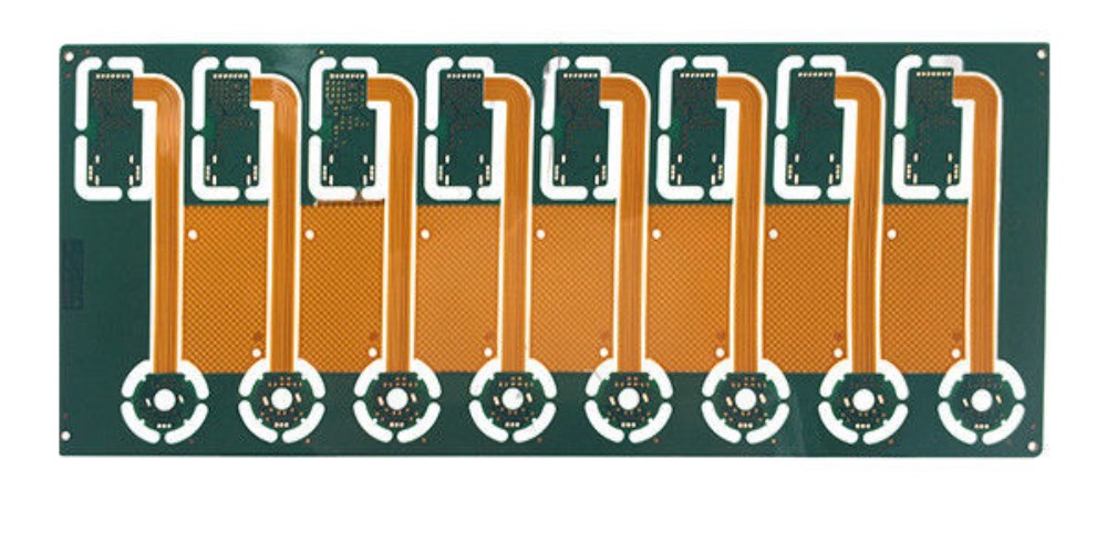
Flexible printed circuit boards (flex PCBs or flex circuits) are a type of PCB made of flexible dielectric materials such as polyimide or polyester. Unlike rigid PCBs, flex PCBs can be bent and flexed to fit into tight or moving spaces in electronic devices.
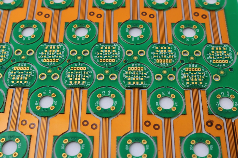
Coverlay is a thin, flexible dielectric material laminated over the surface of a flex PCB to provide electrical insulation, protect circuitry, and strengthen the board. Selecting the right type of coverlay and using proper coverlay processing techniques is critical for a robust, reliable flex PCB design.
In this comprehensive guide, we will cover:
- Benefits of using coverlay on flex PCBs
- Coverlay material options
- Coverlay lamination process
- Coverlay openings and tolerances
- Coverlay design rules and layout considerations
- Coverlay defects to avoid
- Testing and inspection of coverlay
- Coverlay repair and rework
Properly integrating coverlay into your flex PCB design will improve reliability, facilitate assembly, and reduce costs.
Why Use Coverlay on Flexible PCBs?
There are several important benefits provided by coverlay on flex circuits:
Electrical Insulation
Coverlay provides electrical insulation between traces and components on the flex PCB. This helps prevent short circuits when the board is flexed. The dielectric film prevents conductors on opposite sides of the flex from making accidental contact.
Environmental and Mechanical Protection
The coverlay coating safeguards the flex board from mechanical abrasion, chemical contamination, and other environmental hazards. This allows the PCB to be used in more demanding conditions.
Stiffening and Support
Coverlay builds up the thickness of the flex circuit to provide additional stiffness and ruggedness. This makes the PCB more durable and resistant to cracking.
Component Spacing
During assembly, coverlay helps provide accurate spacing between surface mount components. This facilitates automated pick-and-place equipment.
Improved Appearance
Coverlay provides a uniform surface finish over the entire flex board. This gives the assembled PCB a more refined, streamlined appearance.
Enhanced Assembly
Coverlay allows solder paste, adhesives, and other assembly materials to be applied over the entire surface of the PCB. The dielectric film also helps provide mounting adhesion for components.
Coverlay Material Options
Several types of coverlay materials are used for flex PCB applications:
Polyimide
Polyimide film provides the highest heat resistance and mechanical strength. The most common thickness is 1-2 mil. Polyimide coverlay withstands soldering temperatures over 400°C. It has excellent chemical resistance. Polyimide has a amber-gold color.
Polyester
Polyester (PET) coverlay has good dielectric properties, flexibility, and tensile strength. It is more economical than polyimide. Polyester has a lower maximum temperature of 150°C. It is available from 0.5 to 3 mil thickness. Polyester film is clear or semi-transparent.
Liquid Photoimageable
Liquid photoimageable coverlay can be applied by spray coating or screen printing. It is exposed and developed like a standard photoresist. LPI coverlay is typically 1-2 mil thick when cured. It provides good resolution for openings but has less physical strength than polyimide or polyester films.
Silicone
Silicone rubber coverlay has very high flexibility and a wide temperature range. It provides excellent protection against mechanical stresses. The main drawbacks are poorer electrical characteristics and relatively high cost. Silicone coverlays are typically 2-4 mil thick.
In general, polyimide provides the best performance for most rigid-flex PCB designs. Polyester is suitable for more cost-sensitive applications with lower temperature requirements. LPI and silicone coverlays are used for specialized requirements.
Coverlay Lamination Process
For polyimide and polyester coverlay films, the attachment process is similar to laminating layers of a multilayer PCB. There are four primary steps:
Surface Preparation
The flex PCB surface must be thoroughly cleaned before applying coverlay. Any contamination can prevent proper adhesion. A chemical etchant removes oxidation and activates the surface. Plasma cleaning may also be used.
Adhesive Application
A thin layer of acrylic, epoxy, or polyurethane adhesive is applied over the board surface. The adhesive may be spray coated, roller coated, or screen printed on the PCB. The adhesive helps firmly bond the coverlay to the substrate.
Coverlay Attachment
The coverlay film is carefully aligned over the flex board and then laminated together under heat and pressure. Typical lamination temperature is 180-200°C. The adhesive cures to form a strong bond between the coverlay and flex dielectric layers.
Trimming
Once cured, the coverlay is trimmed flush with the PCB outline using a precision router. Corner rounding, bevels, or other edge profiling may also be added.
Careful process controls during lamination are vital to prevent wrinkles, bubbles, delamination, or other defects. Vacuum lamination or autoclave pressing produces the highest quality coverlay layer.
Creating Coverlay Openings
To access testpoints and allow components to be mounted, openings must be created in the coverlay where needed. There are two main methods:
Laser Ablation
A CO2 laser can be used to ablate openings in polyimide and polyester coverlay materials. The laser vaporizes the coverlay to expose selected areas of the flex circuitry. Laser systems provide high precision and productivity.
Mechanical Routing
Openings can also be routed out using mechanical drills or micro cutters. The diameter must be larger than the size of the exposed feature to allow for positional tolerances. Mechanical routing is simpler but lacks the accuracy of lasers.
Typical coverlay opening tolerances are:
- Laser ablation: ±0.05 mm
- Mechanical routing: ±0.10 mm
Maintaining tight control of opening locations and dimensions is critical for a successful coverlay layer.
Coverlay Design Rules and Layout
To ensure proper integration of the coverlay layer, designers should follow these key guidelines:
- Keep all circuitry a minimum 2-3 mm from flex PCB edges underneath coverlay areas. This prevents risk of tearing during lamination.
- Avoid placing coverlay over large copper planes. The adhesive bond may be weaker.
- Use tie downs and stiffeners under components to reduce stress on coverlay.
- Include fiducials for precise alignment of coverlay artwork.
- Allow 1 mm clearance around coverlay openings.
- Minimize the number of individual coverlay openings where possible. -Specify coverlay thickness, opening dimensions, and tolerances on fabrication drawings.
- Work closely with your PCB manufacturer to determine optimal coverlay design parameters.
Careful layout and planning of the coverlay layer based on these guidelines will result in a more robust, reliable flex circuit assembly.
Common Coverlay Defects
Some potential quality issues can occur with coverlay if not properly addressed:
Wrinkling
Wrinkles in the coverlay film appear as ripples across the surface. They are caused by inadequate lamination pressure, temperature, or venting. Wrinkles can lead to cracked coverlay and open circuits.
Delamination
Partial separation of the coverlay film from the substrate is known as delamination. It stems from poor surface prep, contamination, or weak adhesive. Delaminated areas lead to cracked coverlay and loss of insulation.
Bubbles
Small air bubbles trapped between the coverlay and flex layer during lamination will cause localized delamination. This impairs dielectric properties.
Incomplete Openings
If coverlay openings for testpoints or components are undersized, lack proper registration, or have ragged edges it will impact assembly and reliability.
Cosmetic Imperfections
Bumps, dents, scratches, discoloration or debris in the coverlay film may be cosmetic in nature but still influence quality perceptions.
Coverlay Testing and Inspection
Several checks help ensure the coverlay meets specifications:
- Dimensions – Measure coverlay thickness and opening sizes in multiple locations.
- Adhesion – Use peel or pull tests to verify strong coverlay bonding.
- Flexibility – Bend samples around a mandrel to confirm coverlay flexibility.
- Dielectric Strength – Apply high voltage to check for insulation integrity.
- Continuity – Probe testpoints to ensure coverlay openings expose contacts.
- Visual – Inspect under magnification for wrinkles, delamination, and other flaws.
It is also important to assess performance under thermal cycling, vibration, bending, and other environmental stressors.
Reworking and Repairing Coverlay
If defects in the coverlay are identified, it is sometimes possible to repair the PCB without complete re-lamination:
- Delaminated areas can be re-adhered using coverlay repair film and localized heat and pressure.
- Wrinkled sections may be flattened out with mechanical pressing.
- Small damaged or missing pieces can be patched with film adhesive.
- Re-ablating openings to proper size is possible but risks conductor damage.
- Repainting or resurfacing the coverlay can salvage cosmetic defects.
However, extensive coverlay issues often require stripping the original layer and re-applying the coverlay entirely. This adds cost and delays. Careful process control during initial fabrication is key to avoiding coverlay rework.
Frequently Asked Questions About Flex PCB Coverlay
Here are answers to some common questions about coverlay for flexible printed circuits:
What are the typical coverlay thicknesses used?
Polyimide, polyester, and liquid photoimageable coverlay are usually 1 to 2 mils thick. Silicone rubber coverlays range from 2 to 5 mils thick. Thicker coverlay provides more insulation and durability but increases flex circuit stiffness.
Can solder mask be used instead of coverlay?
Solder mask lacks the dielectric strength, thickness, and flex resistance for adequate insulation and protection. Solder mask is more prone to cracking when flexed. Coverlay is specifically designed for insulation of flex PCB conductor layers.
Does coverlay increase manufacturing time?
Adding a coverlay layer does require additional processing steps – surface treatment, adhesive application, lamination, and trimming. However, the extra time is worth the reliability and protection benefits coverlay provides.
Can components be mounted on top of coverlay?
It is possible to mount components on coverlay areas, but adhesion may be weaker than attaching directly to the PCB substrate. Use of tie-downs, underfill, or adhesives is recommended to strengthen the bonds.
How are openings created for testpoints?
To access testpoints, small holes are laser ablated or mechanically drilled through the coverlay layer. This exposes the test contact while maintaining insulation around it. Registration of the openings to the testpoint locations is critical.
In summary, the coverlay layer is an integral part of robust flexible PCB designs. When properly integrated into the fabrication process, coverlay provides insulation, protection, and improved manufacturability. Consider the coverlay options and layout guidelines outlined here when designing your next flex circuit assembly.