


Introduction
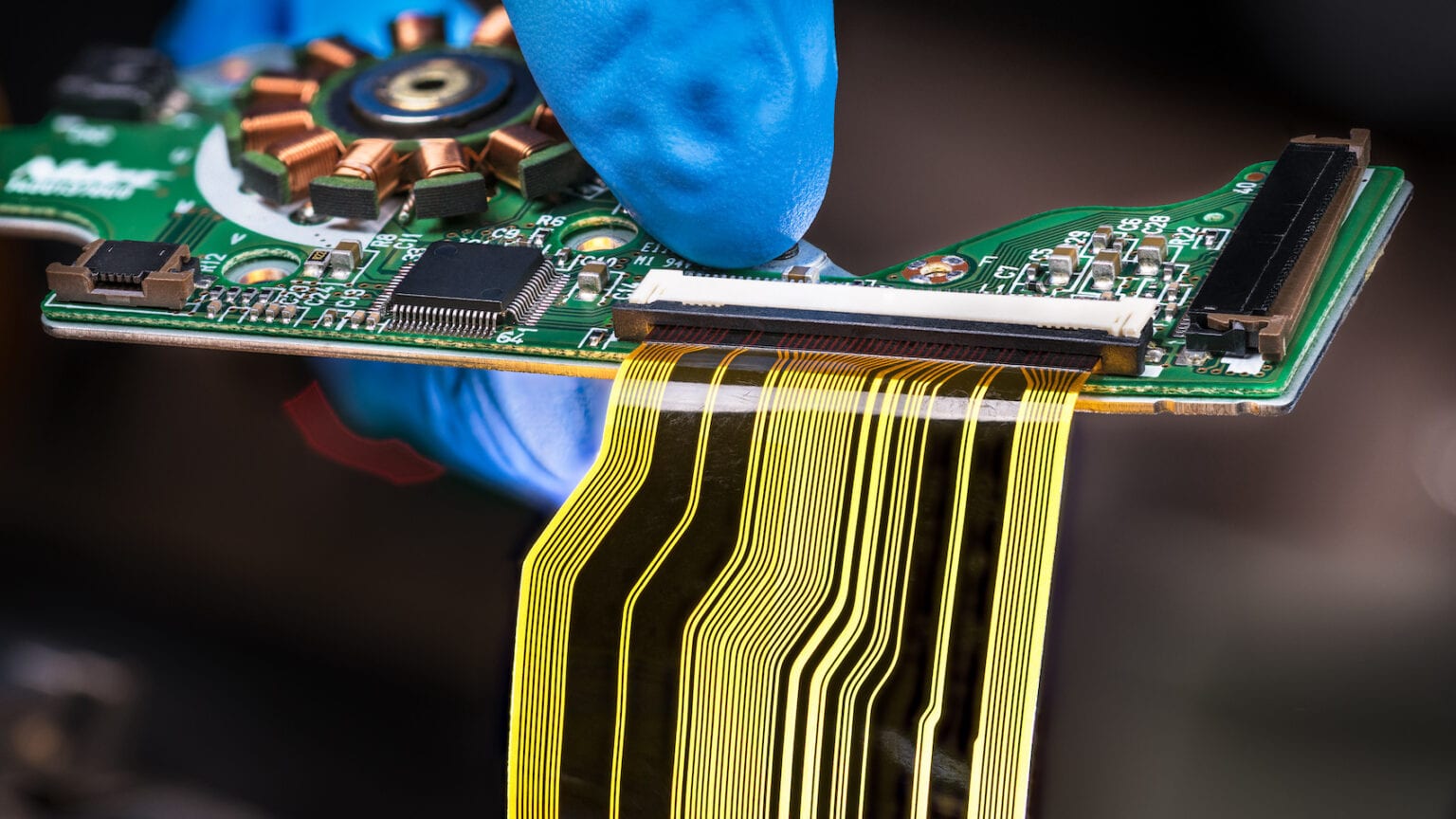
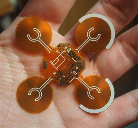
Flexible printed circuit boards (PCBs) are a type of circuit board made with flexible materials that allow the board to bend and flex. Unlike traditional rigid PCBs, flexible PCBs can be folded, twisted, and shaped to fit into tight or irregular spaces. This makes them ideal for use in compact electronic devices like smartphones, wearables, medical devices, and more. However, designing flexible PCBs requires some special considerations compared to rigid boards. In this guide, we’ll cover the key things you need to know about designing flexible PCBs.
Benefits of Flexible PCBs
There are several advantages that flexible PCBs provide over rigid boards:
- Space savings – Flex circuits can fit into tight spaces and bend around components. This allows for smaller and more compact product designs.
- Flexibility – Flexible PCBs can bend, fold, twist, and conform to different shapes. This versatility makes them usable in many unique applications.
- Reliability – The materials used in flex PCBs make them very durable and resistant to cracking or breaking under bending stresses.
- Lightweight – Flexible PCB substrates are thinner and lighter in weight than rigid boards. This is important for portable devices.
- Cost savings – Using a flex PCB with fewer layers can reduce costs compared to using multiple rigid PCBs.
- Improved aesthetics – Circuits can be wrapped around and hidden from view.
Flexible PCB Materials
The most common materials used in the construction of flex PCBs are:
- Polyimide (PI) – This plastic-based film offers excellent heat resistance and mechanical strength. Polyimide is the most widely used flex PCB substrate. Common brands are Kapton and Apical.
- Polyester (PET) – More economical option but with lower maximum temperature rating than polyimide. Often used for simpler low-temperature applications.
- Polyethylene Naphthalate (PEN) – Similar properties as polyimide but even more temperature resistant, at up to 180°C. Used for circuits requiring exposure to high temperatures.
- Fluoropolymers (PTFE) – Superior chemical resistance with a high melting point above 260°C. Useful when flex PCBs are exposed to harsh chemicals.
The copper traces are typically laminated onto the polymer substrate. Adhesives are used to bond multiple layers together if constructing a multilayer flex PCB.
Design Rules and Constraints
Designing the layout and routing for a flexible PCB comes with some key rules and constraints:
Minimum Bend Radius
- This is the smallest bend radius the PCB can be flexed to without damaging the copper traces.
- The minimum bend radius is typically 3-10x the PCB thickness depending on materials.
- Bending beyond the minimum radius can crack the copper and cause track failure.
Trace Width and Spacing
- Traces must be designed wide enough to carry the required current.
- Trace spacing must prevent shorts between traces when flexed.
- Typical trace/space is minimum 8 mil width / 8 mil spacing.
Stiffener Areas
- Sections that won’t bend need stiffener areas with more copper layers to prevent unwanted flexing.
Layer Stackup
- Must use thin flexible dielectric materials between layers.
- Adhesives must withstand flexing stresses between layers.
- Four-layer flex is common, with inner two layers for power/ground planes.
Component Placement
- Avoid placing heavy components in bend areas.
- Use flat lead components instead of gull-wing.
- Adhere components with flex-grade adhesive.
Flex Cuts
- Flex PCB panels are scored partially through to create flexible hinges between sections.
- Cuts made with wheel cutters or lasers.
- Cut depth must be carefully controlled.
Termination Pads
- Pads should be rounded to avoid point stress concentrations.
- May require special reinforcement for durability.
By following these kinds of design criteria, a flexible PCB can be successfully engineered to meet the unique reliability requirements of dynamic flexing applications.
Flex-to-Rigid PCBs
Often, a design will incorporate both flexible and rigid PCB sections. There are a few common ways this can be achieved:
- Discrete flex + rigid PCBs – Separate rigid and flex PCBs joined by connectors or soldered joints. Provides modular approach.
- Integrated flex-rigid – Combines flex and rigid sections into one PCB with flexible “hinges” joining rigid segments. Requires special manufacturing.
- Rigid-flex – Layers of rigid board materials laminated together with flexible laminate layers. Allows high density with inner flexible layers.
- Flex board with stiffener – Flexible PCB bonded to a rigid stiffening plate or frame in select areas. Low cost approach.
The right flex-rigid approach depends on the complexity, spacing, alignment needs, and other requirements.
Flex PCB Layout Tips
Here are some helpful tips when laying out the design of a flexible PCB:
- Minimize the number of bends to reduce stress.
- Avoid sharp/tight bends. Use larger bend radii when possible.
- Route traces perpendicular to the bend axis at flex points.
- Use comb patterns on long trace runs to provide flexibility.
- Plan ahead where components will mount relative to bends.
- Place connectors at the ends of rigid sections.
- Keep rigid sections short, under 40-50mm long if possible.
- Utilize both sides of the PCB for routing to reduce layers.
- Add generous corner radii and non-copper margins.
- Indicate on the silkscreen where flexing occurs and directions.
Following flex PCB layout best practices will help ensure the design can survive the mechanical stresses of continuous bending motion after assembly.
Flex PCB Prototyping and Testing
When designing a new flex circuit, it’s important to prototype and test the design. Some recommendations include:
- Review layout in CAD software bend tools to check stresses
- Build extra flex boards for testing different bend radiuses
- Perform test bends with sample boards to validate minimum radius
- Environmental stress test with repeated flexing cycles
- Thermal cycling from minimum to maximum temperatures
- Shock and vibration testing while flexed
- Electrical testing while flexed at minimum and maximum positions
By using both physical and electrical testing methods, designers can verify that the flex PCB can meet the reliability requirements of the application.
Applications of Flexible PCBs
Due to their unique properties, flexible PCBs are used in a wide range of products:
Consumer Electronics
- Smartphones
- Laptops
- Tablets
- Digital cameras
- Wearable devices
Medical
- Hearing aids
- Pacemakers
- Prosthetics
- Patient monitoring
Automotive
- Electronics under the hood
- Mirror adjustments
- Gear shifters
- Lighting
Industrial
- Robotics
- Motors and drives
- POS terminals
- Machine controls
Aerospace/Military
- Guidance systems
- Avionics
- Radar arrays
- Missiles
Pretty much any application where saving space, moving/flexing parts, or resisting vibration is a key consideration can benefit from the unique advantages of flexible circuits.
As flexible PCB technology continues advancing, the applications and market adoption will only increase.
Flexible PCB Manufacturing
Producing flexible PCBs requires specialized manufacturing processes tailored to the properties of flex materials. Here is a high-level overview:
Lamination
- Layers of adhesive-coated flexible dielectric and copper foil are stacked up in the press.
- Heat and pressure bonds the layers together into a solid laminate sheet.
Imaging
- Photoresist coatings are applied on copper layers.
- The artwork patterns are exposed on each layer.
Etching
- Etchants remove unwanted copper to leave behind the desired traces.
- Etch resists maintain the artwork patterns.
Coverlay or Solder Mask
- A protective coating is laminated or printed over traces.
- Openings left for solder pads and probe points.
Finishing
- Various surface finishes like ENIG or immersion silver applied.
- Improves solder joint reliability.
Singulation
- Individual PCBs are routed out from the full laminate panels.
- Allows further processing of each flex board.
Assembly
- Components added by soldering or conductive adhesive.
- Often requires special fixturing to control flexing.
There are additional steps with inspection, testing, and quality control throughout the sequence.
Summary
- Flexible PCBs provide many advantages like space savings and improved reliability in bending applications.
- Key design considerations include minimum bend radius, trace dimensions, layer stackup, component placement, and more.
- Prototyping and testing of flex designs is critical to ensure flexibility and reliability requirements are met.
- Flex-rigid PCBs combine flexible sections and rigid regions into one integrated PCB solution.
- Flexible circuits are used in diverse applications ranging from consumer gadgets to advanced medical and aerospace systems.
- Specialized manufacturing processes are tailored to handle flexible materials during PCB production.
By understanding the unique requirements of flexible PCBs, engineers can take full advantage of their benefits in designing the next generation of compact, reliable electronic devices.
Frequently Asked Questions
What are some typical dielectric materials used in flexible PCBs?
Some of the most common flexible PCB substrate materials are polyimide (Kapton), polyester (PET), polyethylene naphthalate (PEN), and fluoropolymers like PTFE. Each has different properties in terms of flexibility, maximum temperature, chemical resistance, and cost.
How many traces can you fit on a flex PCB?
A two-layer flex PCB with minimum 8 mil trace/space rules could fit over 150 traces in a 1″ width. With smaller traces using tighter rules, over 300 traces is possible in 1″. For higher densities, 4-layer or more flex PCBs are used.
Can components be mounted on both sides of a flexible PCB?
Yes, components can be surface mounted onto both sides of a flex PCB. The components need to be small with flat terminations. Additionally, the component adhesive needs to withstand flexing and the board may require stiffeners in the component areas.
Is it possible to make multilayer flex PCBs?
Multilayer flex PCBs with 4, 6 or more layers can be constructed. This requires bonding thin flexible dielectric layers together using adhesive. Inner layers are commonly used for power and ground to simplify routing, similar to rigid multilayer boards. High density interconnects are possible with flexible multilayers.
Can flex PCBs be tested using standard techniques?
Yes, common electrical test methods like in-circuit test (ICT), flying probe, and boundary scan work well for verifying flex PCB assemblies. The fixtures may need to accommodate for the board flexing during test. Environmental stress screening under dynamic flexing provides additional reliability testing.