
-
What is high density PCB board?
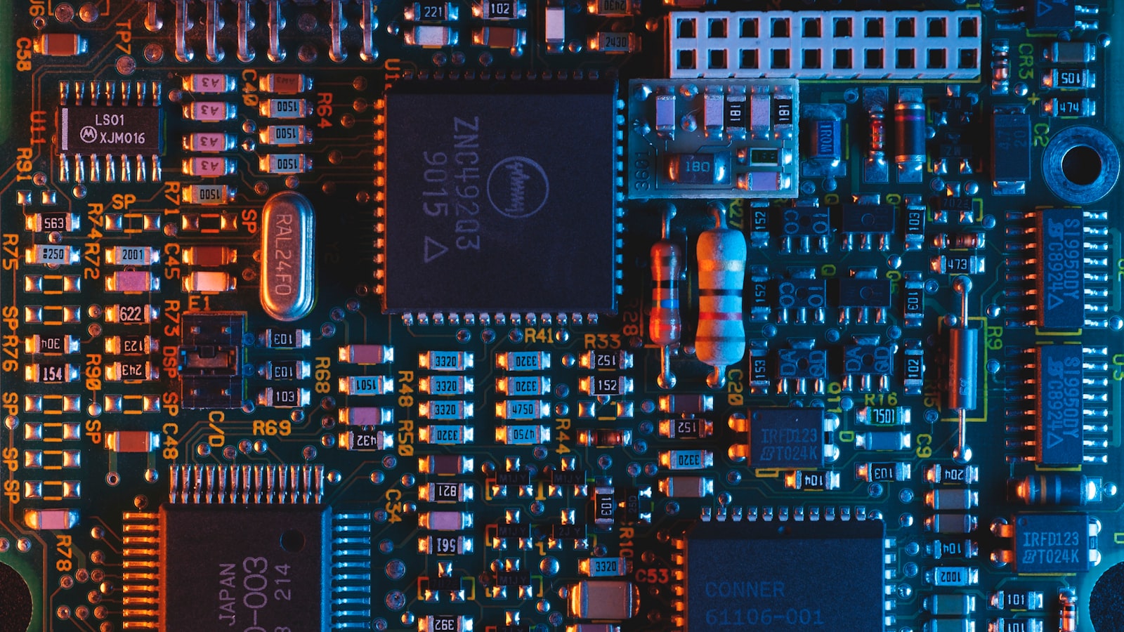
Key Features of HDI PCBs HDI PCBs have several distinct features that set them apart from traditional PCBs: Smaller vias and pads Finer trace widths and spacings Multiple layers (typically 8 or more) Blind and buried vias Microvias (vias with a diameter less than 150 microns) These features enable HDI PCBs to pack more functionality…
-

How to make a LED PCB?
Introduction to LED PCBs A LED PCB (Printed Circuit Board) is a custom-designed circuit board that incorporates LEDs (Light Emitting Diodes) for various lighting applications. These PCBs are widely used in electronics projects, signage, automotive lighting, and more. Creating a LED PCB involves several steps, including circuit design, PCB layout, component selection, and assembly. In…
-

What Is the Difference Between PCBA and PCB?
What is a PCB? PCB stands for “printed circuit board.” It is the base board that provides electrical connections and mechanical support for electronic components. A PCB starts as a non-conductive substrate, typically made of fiberglass (FR4), with a thin layer of copper foil laminated to one or both sides. The copper is etched away…
-

Why Choose RayMing Assembly service for Your PCB Requirements?
What are PCB Assembly Services? PCB assembly services encompass the process of transforming a bare PCB into a fully functional circuit board by soldering electronic components onto its surface. This process involves several stages, including: Solder Paste Application Component Placement Reflow Soldering Inspection and Testing Professional PCB assembly service providers, like RayMing, utilize state-of-the-art equipment…
-
What are standard PCB thicknesses?
Understanding PCB Thickness PCB thickness refers to the distance between the top and bottom surfaces of the board, excluding any additional layers such as solder mask or silkscreen. The thickness of a PCB is typically measured in either inches or millimeters. Common PCB Thickness Units Inches (e.g., 0.031″, 0.062″) Millimeters (e.g., 0.8mm, 1.6mm) It’s important…
-

Are printed circuit boards made in the USA?
The History of PCB Manufacturing in the USA The concept of the printed circuit board can be traced back to the early 20th century when patents for similar ideas were filed by inventors like Thomas Edison and Albert Hanson. However, it wasn’t until the 1940s that PCBs began to be used extensively in electronic devices,…
-
What is a PCB designer?
The Role of a PCB Designer The primary responsibility of a PCB designer is to create a functional and efficient layout of electronic components on a printed circuit board. They work closely with electrical engineers and other stakeholders to understand the requirements of the device and develop a design that meets those needs. Key Responsibilities…
-
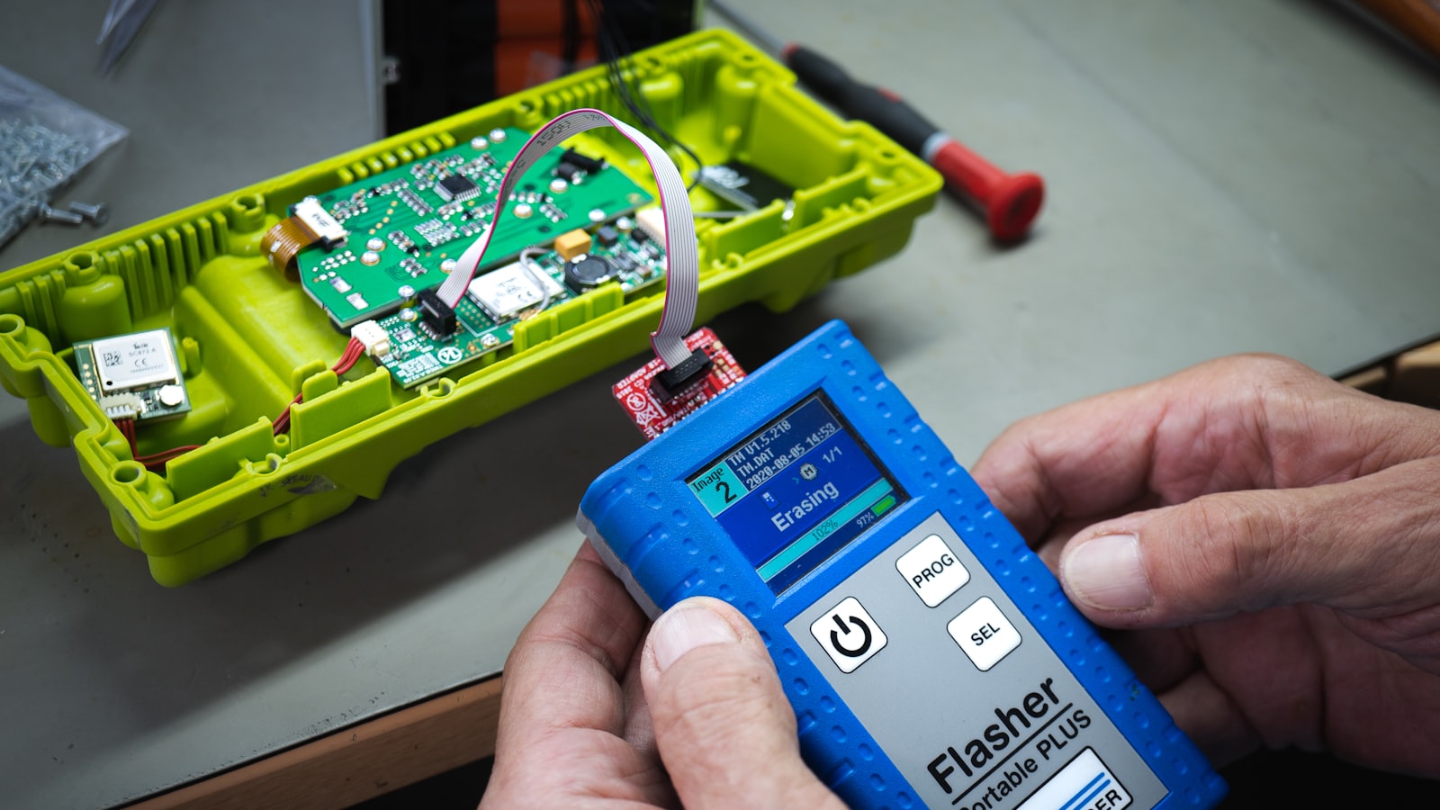
What is PCB prototyping?
The Importance of PCB Prototyping PCB prototyping is crucial for several reasons: Design Validation: Prototyping allows designers to physically test their PCB layouts and ensure that they function as intended. This helps identify any design flaws or potential issues early in the development process. Cost Savings: By identifying and resolving issues during the prototyping phase,…
Blog
Archive
Categorise
Recent Posts
- Common Mode Choke Selection: A Comprehensive Guide
- Common Fab and Assembly Design Errors To Avoid – AltiumLive 2024
- Commodore 128 Principal Engineer, Bil Herd on Best Practices for Learning a New CAD Tool
- Collecting All the Pieces You Need: What is a Bill of Materials?
- Collaborative Design Software: Create PCB Schematic Symbols for any Component