


What is PCB strain relief and why is it important?
PCB strain relief is a method of reducing mechanical stress on electrical connections between printed circuit boards (PCBs) and wires or cables. It is important because it helps prevent damage to the connections caused by pulling, twisting, or other physical forces that can occur during manufacturing, installation, or use of the PCB Assembly.
When wires or cables are connected directly to a PCB without strain relief, any movement or stress on the wires can transfer directly to the solder joints or other connection points on the board. Over time, this can cause the connections to weaken or break, leading to electrical failures or intermittent problems.
Strain relief methods help to absorb or redirect these forces away from the connections, reducing the risk of damage and improving the reliability and longevity of the PCB assembly.
Common types of PCB strain relief
There are several common methods used for PCB strain relief, including:
- Cable ties or clamps: These are simple devices that wrap around the wire or cable and attach to the PCB or enclosure, holding the wire in place and absorbing some of the stress.
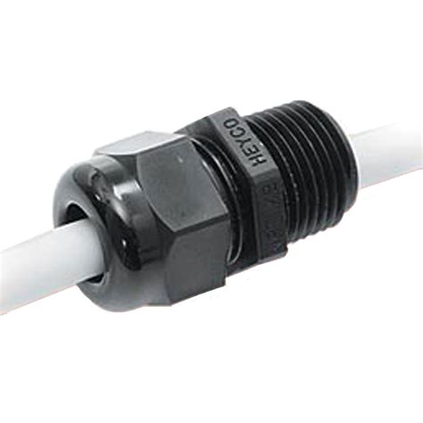
- Strain relief connectors: These are specialized connectors that have built-in strain relief features, such as a flexible boot or clamp that grips the wire.
- Adhesive-backed cable mounts: These are small plastic or metal mounts that stick to the PCB or enclosure and have a slot or hole for the wire to pass through, providing a secure anchor point.
- Molded strain relief: This involves molding a plastic or rubber sleeve around the wire at the point where it enters the PCB or connector, creating a strong, flexible transition that absorbs stress.
- Board-edge connectors: These are connectors that mount on the edge of the PCB and have a built-in strain relief mechanism, such as a clamping bar or spring-loaded contacts.
| Method | Advantages | Disadvantages |
|---|---|---|
| Cable ties or clamps | Inexpensive, easy to install | May not provide enough strain relief for heavy or stiff wires |
| Strain relief connectors | Provides good strain relief, easy to use | May be more expensive than other methods |
| Adhesive-backed cable mounts | Easy to install, low profile | May not work well with heavy or stiff wires |
| Molded strain relief | Provides excellent strain relief, can be customized | Requires special tooling, may be more expensive |
| Board-edge connectors | Provides good strain relief, easy to use, saves board space | May be more expensive, limited to certain connector types |
Designing for PCB strain relief
When designing a PCB assembly that requires strain relief, there are several factors to consider:
- Wire or cable type: The size, stiffness, and weight of the wires or cables will affect the type and amount of strain relief needed.
- Expected use environment: The expected level of physical stress on the wires, such as from vibration, shock, or repeated flexing, will influence the strain relief design.
- Available space: The size and location of the strain relief method must fit within the available space on the PCB or enclosure.
- Manufacturing process: The strain relief method must be compatible with the PCB assembly process, such as soldering, potting, or overmolding.
- Cost: The cost of the strain relief components and any additional manufacturing steps must be considered in the overall design budget.
Best practices for PCB strain relief design
Here are some best practices to follow when designing PCB strain relief:
- Use the appropriate strain relief method for the wire or cable type and expected use environment.
- Locate the strain relief as close as possible to the connection point on the PCB to minimize the unsupported length of wire.
- Allow enough slack in the wire between the strain relief and the connection point to avoid putting stress on the connection during assembly or use.
- Consider using multiple strain relief methods in series for added protection, such as a cable tie followed by a molded strain relief.
- Test the strain relief design under expected use conditions to ensure it provides adequate protection and does not interfere with the function of the PCB assembly.

Examples of PCB strain relief applications
PCB strain relief is used in a wide variety of applications, from consumer electronics to industrial equipment. Here are a few examples:
- Automotive electronics: PCBs used in vehicles are subject to high levels of vibration and temperature extremes, making strain relief critical for reliable operation. Common methods include molded strain reliefs on wiring harnesses and board-edge connectors with built-in strain relief.
- Medical devices: PCBs used in medical equipment must be highly reliable and able to withstand repeated use and cleaning. Strain relief methods such as adhesive-backed cable mounts and strain relief connectors are commonly used to protect wiring connections.
- Industrial controls: PCBs used in industrial Control Panels and equipment are often subject to heavy use and harsh environments. Cable ties, clamps, and molded strain reliefs are used to protect wiring connections and ensure reliable operation.
- Consumer electronics: PCBs used in products such as smartphones, laptops, and televisions must be able to withstand daily use and occasional drops or impacts. Strain relief methods such as adhesive-backed cable mounts and molded strain reliefs are used to protect delicate wiring connections.

Frequently Asked Questions (FAQ)
- Q: What is the most common method of PCB strain relief?
A: Cable ties and clamps are the most common method of PCB strain relief due to their low cost and ease of installation. - Q: Can strain relief be added to an existing PCB assembly?
A: Yes, strain relief can often be added to an existing PCB assembly using methods such as cable ties or adhesive-backed cable mounts, as long as there is sufficient space and access to the wiring connections. - Q: How much strain relief is needed for a given application?
A: The amount of strain relief needed depends on factors such as the size and stiffness of the wires, the expected use environment, and the level of reliability required. Testing under expected use conditions can help determine the appropriate level of strain relief. - Q: Can strain relief be used with Flexible PCBs?
A: Yes, strain relief can be used with flexible PCBs, but the methods used may need to be adapted to account for the flexibility of the board. Adhesive-backed cable mounts and molded strain reliefs are common choices for flexible PCBs. - Q: Are there any standards or regulations governing PCB strain relief?
A: There are no specific standards or regulations governing PCB strain relief, but there are general guidelines and best practices that should be followed to ensure reliable operation. Industry standards such as IPC-A-610 and IPC/WHMA-A-620 provide guidance on cable and Wire Harness assembly, including strain relief methods.

Conclusion
PCB strain relief is an important consideration in the design and manufacturing of reliable electronic assemblies. By understanding the different methods available and following best practices for design and installation, engineers and manufacturers can ensure that their PCB assemblies are protected from damage caused by physical stress on wiring connections.
While there is no one-size-fits-all solution for PCB strain relief, selecting the appropriate method based on the specific application and use environment can help to optimize reliability, longevity, and cost-effectiveness. As electronic devices continue to become smaller, more complex, and more widely used in demanding environments, the importance of effective PCB strain relief will only continue to grow.