

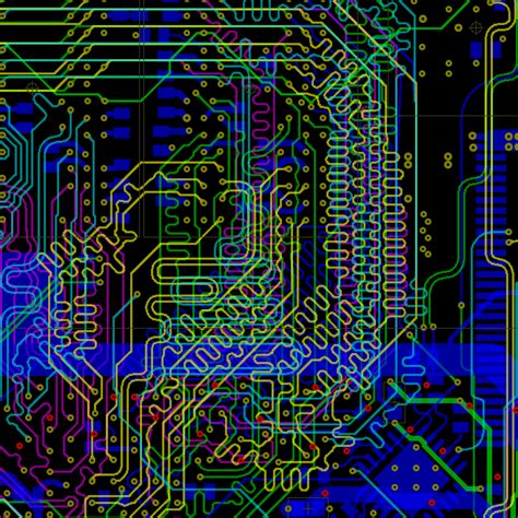
Introduction to PCB topology
Printed Circuit Board (PCB) topology plays a crucial role in the design and performance of high-speed electronic systems. As signal speeds continue to increase, the layout and routing of traces on a PCB become increasingly important to ensure signal integrity, minimize electromagnetic interference (EMI), and optimize overall system performance. In this article, we will delve into the key aspects of high-speed PCB layout topology, exploring best practices, design considerations, and techniques to achieve optimal results.
Understanding High-Speed Signals
What are High-Speed Signals?
High-speed signals are electrical signals that have fast rise and fall times, typically in the range of picoseconds to nanoseconds. These signals are commonly found in modern electronic systems, such as high-speed digital interfaces, high-frequency analog circuits, and high-bandwidth communication systems. Examples of high-speed signals include:
- PCIe (Peripheral Component Interconnect Express)
- USB 3.0 and above
- HDMI (High-Definition Multimedia Interface)
- SATA (Serial ATA)
- DDR (Double Data Rate) memory interfaces
Signal Integrity Challenges
As signal speeds increase, several signal integrity challenges arise that can impact the quality and reliability of the transmitted data. These challenges include:
- Reflections: When a signal encounters an impedance discontinuity, such as a change in trace width or a connector, a portion of the signal reflects back towards the source. These reflections can cause signal distortion, overshoot, and undershoot.
- Crosstalk: Crosstalk occurs when a signal on one trace induces unwanted voltage or current on a neighboring trace. This can lead to signal interference and data corruption.
- Electromagnetic Interference (EMI): High-speed signals can radiate electromagnetic energy, causing interference with other electronic devices. Proper PCB layout techniques are essential to minimize EMI and ensure compliance with electromagnetic compatibility (EMC) regulations.
- Timing Skew: Timing skew refers to the difference in arrival times of signals at their respective destinations. Excessive timing skew can cause data errors and limit the maximum operating frequency of the system.

PCB Stackup and Material Selection
Choosing the Right PCB Stackup
The PCB stackup refers to the arrangement of copper layers and dielectric materials that make up the PCB. Selecting an appropriate stackup is crucial for high-speed design. Consider the following factors when choosing a PCB stackup:
- Number of Layers: Determine the number of layers required based on the complexity of the design, signal density, and routing requirements. High-speed designs often benefit from additional layers to provide dedicated power and ground planes, as well as separate signal layers for critical traces.
- Layer Arrangement: Arrange the layers to optimize signal integrity and minimize crosstalk. Common practices include:
- Placing power and ground planes adjacent to each other to provide a low-impedance return path for high-speed signals.
- Alternating signal layers with ground planes to provide shielding and reduce crosstalk.
- Routing critical signals on inner layers to minimize external noise coupling.
- Dielectric Material: Choose a dielectric material with suitable electrical properties, such as low dielectric constant (Dk) and low dissipation factor (Df), to minimize signal loss and maintain signal integrity.
Material Selection
The choice of PCB material is critical for high-speed designs. The dielectric material properties directly impact signal propagation, loss, and impedance control. Some commonly used high-speed PCB materials include:
| Material | Dk | Df | Applications |
|---|---|---|---|
| FR-4 | 4.3 | 0.022 | General-purpose, cost-effective |
| Rogers RO4350B | 3.48 | 0.0037 | High-frequency, low-loss |
| Isola I-Tera MT40 | 3.45 | 0.0035 | High-speed digital, automotive, aerospace |
| Nelco N4000-13EP | 3.7 | 0.009 | High-speed digital, aerospace, defense |
When selecting a PCB material, consider the following factors:
- Dielectric constant (Dk): A lower Dk value results in faster signal propagation and lower signal loss.
- Dissipation factor (Df): A lower Df value indicates lower signal loss and better high-frequency performance.
- Thermal stability: Choose a material with good thermal stability to minimize dimensional changes due to temperature variations.
- Cost: Balance the performance requirements with the cost constraints of the project.

Controlled Impedance and Trace Routing
Impedance Control
Controlling the characteristic impedance of traces is essential for maintaining signal integrity in high-speed designs. Impedance mismatches can lead to reflections, signal distortion, and reduced noise margin. To achieve controlled impedance, consider the following:
- Trace Width and Spacing: Adjust the trace width and spacing to achieve the desired characteristic impedance. Wider traces result in lower impedance, while narrower traces result in higher impedance. Use PCB design tools with Impedance Calculators to determine the optimal trace dimensions.
- Dielectric Thickness: The thickness of the dielectric material between the signal trace and the reference plane (usually ground) affects the characteristic impedance. Thinner dielectrics result in lower impedance, while thicker dielectrics result in higher impedance.
- Reference Planes: Provide uninterrupted reference planes (ground or power) adjacent to the signal traces to maintain a consistent return path and control impedance.
Trace Routing Techniques
Proper trace routing techniques are crucial for minimizing signal integrity issues and ensuring reliable high-speed performance. Consider the following guidelines:
- Length Matching: Match the lengths of traces within a differential pair or a group of related signals to minimize timing skew. Use serpentine routing or meandering techniques to adjust trace lengths as needed.
- Trace Corners: Avoid sharp 90-degree corners in trace routing, as they can cause impedance discontinuities and reflections. Use 45-degree angles or curved traces to smooth out the transitions.
- Trace Separation: Maintain adequate separation between traces to minimize crosstalk. The spacing between traces should be based on the signal speed, trace geometry, and dielectric properties. Use PCB design tools to calculate the optimal trace spacing.
- Via Placement: Minimize the use of vias in high-speed traces, as they introduce impedance discontinuities and can cause signal reflections. When vias are necessary, place them strategically to minimize their impact on signal integrity.

Power Distribution Network (PDN) Design
Power Plane Placement
A robust power distribution network (PDN) is essential for providing clean and stable power to high-speed components. Consider the following guidelines for power plane placement:
- Solid Power and Ground Planes: Use solid power and ground planes instead of split planes or gridded planes. Solid planes provide low-impedance power distribution and help minimize voltage fluctuations.
- Plane Capacitance: Take advantage of the natural capacitance between power and ground planes to provide high-frequency decoupling. Thin dielectric layers between the planes increase the capacitance and improve high-frequency performance.
- Plane Separation: Maintain adequate separation between power planes of different voltages to prevent electromagnetic coupling and ensure electrical isolation.
Decoupling and Bypass Capacitors
Decoupling and bypass capacitors play a critical role in maintaining power integrity and reducing noise in high-speed systems. Consider the following practices:
- Placement: Place decoupling capacitors as close as possible to the power pins of high-speed components. This minimizes the inductance in the power path and provides effective high-frequency decoupling.
- Value Selection: Use a combination of capacitor values to provide broadband decoupling. Smaller capacitors (e.g., 0.01 µF) handle high-frequency noise, while larger capacitors (e.g., 1 µF) handle lower-frequency noise.
- Mounting: Use surface-mount capacitors with low equivalent series inductance (ESL) to minimize the inductance in the decoupling path. Orient the capacitors to minimize the loop area between the capacitor and the power/ground planes.
EMI Reduction Techniques
Shielding
Shielding is an effective technique to reduce electromagnetic interference (EMI) in high-speed systems. Consider the following shielding methods:
- Metal Enclosures: Use metal enclosures to provide overall shielding for the PCB. Ensure proper grounding of the enclosure to the PCB ground plane.
- Local Shielding: Apply local shielding techniques, such as metal cans or shield cages, to specific high-noise components or sensitive circuits. This helps contain EMI at the source and prevents it from coupling to other parts of the system.
- Gaskets and Seals: Use conductive gaskets and seals to ensure continuous electrical contact between the shielding components and the PCB. This prevents EMI leakage through gaps and openings.
Grounding and Isolation
Proper grounding and isolation techniques are essential for minimizing EMI and ensuring signal integrity. Consider the following guidelines:
- Ground Plane: Provide a solid and continuous ground plane on the PCB to create a low-impedance return path for high-speed signals. Avoid splitting the ground plane or creating multiple ground domains unless necessary for noise isolation.
- Ground Stitching: Use ground stitching vias to provide a low-impedance connection between ground planes on different layers. Place ground stitching vias near high-speed signals and connectors to minimize ground bounce and EMI.
- Isolation: Implement proper isolation techniques, such as using separate power and ground planes for noise-sensitive circuits, to prevent interference from noisy components. Use ferrite beads or common-mode chokes to suppress high-frequency noise on power lines or communication interfaces.
Simulation and Verification
Signal Integrity Simulation
Signal integrity simulation is an essential step in validating the high-speed PCB layout before fabrication. Use specialized simulation tools to analyze the following:
- Impedance Matching: Verify that the trace impedances match the desired characteristic impedance and identify any impedance discontinuities that may cause reflections.
- Crosstalk Analysis: Simulate the crosstalk between adjacent traces and identify potential signal integrity issues. Adjust trace spacing or implement shielding techniques as needed.
- Eye Diagram Analysis: Generate eye diagrams to assess the quality of the high-speed signals. Ensure that the eye opening is sufficiently wide and the signal levels are within the required margins.
EMC Simulation
Electromagnetic compatibility (EMC) simulation helps predict and mitigate EMI issues in the PCB design. Use EMC simulation tools to analyze the following:
- Radiated Emissions: Simulate the radiated emissions from the PCB and identify potential EMI sources. Adjust the layout, implement shielding, or apply filtering techniques to reduce emissions.
- Susceptibility Analysis: Evaluate the susceptibility of the PCB to external electromagnetic fields and identify potential coupling paths. Implement protective measures, such as shielding or filtering, to improve the system’s immunity to EMI.
Best Practices and Design Guidelines
- Keep high-speed traces as short as possible to minimize signal reflections and attenuation.
- Route high-speed traces on inner layers, sandwiched between ground planes, to provide shielding and reduce external noise coupling.
- Avoid routing high-speed traces parallel to each other for long distances to minimize crosstalk. If parallel routing is unavoidable, maintain sufficient spacing or use guard traces.
- Use differential signaling for high-speed interfaces to improve noise immunity and reduce EMI.
- Terminate high-speed traces with appropriate resistors to match the characteristic impedance and minimize reflections.
- Provide sufficient power and ground pins for high-speed components to ensure a low-impedance power distribution network.
- Use ground return vias adjacent to high-speed signal vias to minimize inductance and provide a clean return path.
- Implement ESD (electrostatic discharge) protection measures, such as using TVS (transient voltage suppressor) diodes or ESD Protection ICs, to protect sensitive high-speed components.
- Follow the manufacturer’s layout guidelines and recommendations for specific high-speed components or interfaces.
- Perform thorough signal integrity and EMC simulations to validate the design before fabrication, and conduct real-world testing to ensure compliance with industry standards and regulations.
FAQs
- Q: What is the importance of impedance control in high-speed PCB design?
A: Impedance control is crucial in high-speed PCB design to ensure proper signal integrity and minimize reflections. By matching the characteristic impedance of the traces to the source and load impedances, signal reflections are minimized, preventing signal distortion and maintaining signal quality. - Q: How does the choice of PCB material affect high-speed performance?
A: The choice of PCB material significantly impacts high-speed performance. Materials with lower dielectric constant (Dk) and dissipation factor (Df) are preferred for high-speed designs. Lower Dk materials allow for faster signal propagation, while lower Df materials reduce signal loss and maintain signal integrity at higher frequencies. - Q: What is the purpose of length matching in high-speed trace routing?
A: Length matching is essential in high-speed trace routing to minimize timing skew between signals. By ensuring that the traces within a differential pair or a group of related signals have equal lengths, the arrival times of the signals at their respective destinations are synchronized. This prevents data errors and ensures reliable high-speed communication. - Q: How can I reduce crosstalk between high-speed traces?
A: To reduce crosstalk between high-speed traces, consider the following techniques: - Increase the spacing between adjacent traces.
- Use guard traces or ground traces between sensitive signals to provide shielding.
- Route high-speed traces on different layers with ground planes in between to minimize electromagnetic coupling.
- Use differential signaling, which has better noise immunity and reduces crosstalk.
- Q: What are some common EMI reduction techniques in high-speed PCB design?
A: Common EMI reduction techniques in high-speed PCB design include: - Shielding: Using metal enclosures, local shielding (e.g., metal cans or shield cages), and conductive gaskets to contain EMI.
- Grounding and isolation: Providing a solid and continuous ground plane, using ground stitching vias, and implementing proper isolation techniques (e.g., separate power and ground planes for noise-sensitive circuits).
- Filtering: Applying filters, such as ferrite beads or common-mode chokes, to suppress high-frequency noise on power lines or communication interfaces.
- Trace routing: Minimizing loop areas, avoiding sharp corners, and providing adequate spacing between high-speed traces and other signals.
Conclusion
High-speed PCB layout topology is a critical aspect of designing reliable and performance-optimized electronic systems. By understanding the principles of signal integrity, selecting appropriate materials, implementing controlled impedance and proper trace routing techniques, designing a robust power distribution network, and applying EMI reduction measures, designers can create PCBs that meet the demanding requirements of high-speed applications.
Simulation and verification play a vital role in validating the design before fabrication, helping to identify and mitigate potential issues early in the development process. By following best practices and industry guidelines, designers can ensure that their high-speed PCBs perform optimally and meet the required specifications.
As signal speeds continue to increase and system complexity grows, staying up-to-date with the latest techniques and technologies in high-speed PCB layout topology becomes increasingly important. Continuous learning, experimentation, and collaboration with experienced designers and industry experts are essential for achieving success in this dynamic field.