

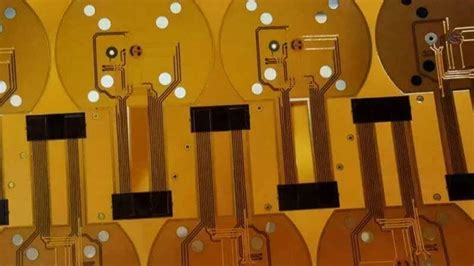
Introduction to Flexible PCB
Flexible printed circuit boards (PCBs) have revolutionized the electronics industry by providing a versatile, lightweight, and durable solution for connecting electronic components. Unlike traditional rigid PCBs, flexible PCBs can bend, twist, and fold to fit into tight spaces and conform to various shapes. This unique property makes them ideal for applications that require compact packaging, enhanced durability, and improved reliability.
In this comprehensive article, we will delve into the world of flexible PCBs, exploring their manufacturing process, advantages, applications, and frequently asked questions. Whether you are an electronics enthusiast, a design engineer, or simply curious about this innovative technology, this article will provide you with valuable insights and knowledge.
What is a Flexible PCB?
A flexible PCB, also known as a flex circuit or flexible printed wiring, is a type of printed circuit board that consists of a thin, flexible substrate with conductive traces and electronic components mounted on its surface. The substrate is typically made of polymeric materials such as polyimide or polyester, which provide excellent flexibility, high temperature resistance, and electrical insulation properties.
Flexible PCBs can be classified into three main categories based on their construction:
- Single-sided flex PCBs: These have conductive traces on only one side of the substrate.
- Double-sided flex PCBs: These have conductive traces on both sides of the substrate, with plated through-holes connecting the two layers.
- Multi-layer flex PCBs: These consist of multiple layers of flexible substrates bonded together, with conductive traces on each layer and interconnections between layers.

Advantages of Flexible PCBs
Flexible PCBs offer several advantages over traditional rigid PCBs, making them the preferred choice for many applications. Some of the key benefits include:
- Flexibility and bendability: Flexible PCBs can bend, twist, and fold to fit into tight spaces and conform to various shapes, enabling more compact and efficient packaging of electronic devices.
- Lightweight and thin: Flex circuits are typically thinner and lighter than rigid PCBs, making them ideal for portable and weight-sensitive applications.
- High reliability: The flexible nature of flex PCBs allows them to withstand vibrations, shocks, and thermal stresses better than rigid PCBs, enhancing the overall reliability of the electronic device.
- Improved signal integrity: Flex circuits can be designed with controlled impedance and shorter signal paths, reducing electromagnetic interference (EMI) and improving signal integrity.
- Cost-effective: In many cases, using flexible PCBs can reduce the overall cost of an electronic device by eliminating the need for connectors, cables, and other hardware.

Applications of Flexible PCBs
Flexible PCBs find applications in a wide range of industries and products, thanks to their unique properties and advantages. Some common applications include:
- Consumer electronics: Smartphones, tablets, laptops, wearables, and other portable devices often use flex circuits to achieve compact and lightweight designs.
- Medical devices: Implantable devices, surgical instruments, and diagnostic equipment rely on flexible PCBs for their reliability, biocompatibility, and ability to conform to body contours.
- Automotive electronics: Flex circuits are used in vehicle dashboards, infotainment systems, and under-the-hood applications due to their durability and resistance to harsh environments.
- Aerospace and defense: Satellites, aircraft, and military equipment employ flexible PCBs for their lightweight, compact, and reliable performance in extreme conditions.
- Industrial automation: Robotics, machine vision systems, and process control equipment use flex circuits for their flexibility and ability to fit into tight spaces.

The Flexible PCB Manufacturing Process
The manufacturing process of flexible PCBs involves several steps, each requiring precision and expertise to ensure the highest quality and reliability. Let’s take a closer look at the key stages of flexible PCB manufacturing.
Step 1: Design and Layout
The first step in the flexible PCB manufacturing process is designing the circuit layout using computer-aided design (CAD) software. The design must consider the specific requirements of the application, such as the size, shape, and flexibility needed. The designer must also ensure that the layout adheres to the design rules and guidelines for flexible PCBs, such as minimum trace width, spacing, and bend radius.
Step 2: Substrate Preparation
Once the design is finalized, the next step is to prepare the flexible substrate. The most common substrate materials for flexible PCBs are polyimide and polyester. The substrate is cleaned and treated to improve its adhesion properties and ensure proper bonding with the conductive traces.
Step 3: Lamination
In this step, the prepared substrate is laminated with a thin layer of copper foil using heat and pressure. The copper foil serves as the conductive material for the traces and pads. For double-sided or multi-layer flex PCBs, multiple layers of substrate and copper foil are laminated together.
Step 4: Patterning and Etching
After lamination, the desired circuit pattern is transferred onto the copper layer using photolithography. A photoresist is applied to the copper surface and exposed to UV light through a photomask containing the circuit pattern. The exposed areas of the photoresist are then developed and removed, leaving the desired pattern on the copper layer.
Next, the unwanted copper is etched away using a chemical etching process, typically with ferric chloride or ammonium persulfate. The remaining photoresist is then stripped off, revealing the final circuit pattern on the flexible substrate.
Step 5: Coverlay Application
To protect the conductive traces and provide electrical insulation, a coverlay film is applied to the flex circuit. The coverlay is typically made of the same material as the substrate and is laminated onto the circuit using heat and pressure. Openings in the coverlay are made to expose the pads for component assembly and interconnections.
Step 6: Surface Finishing
To enhance the solderability and protect the exposed copper pads, a surface finish is applied. Common surface finishes for flexible PCBs include:
- Hot Air Solder Leveling (HASL)
- Electroless Nickel Immersion Gold (ENIG)
- Immersion Silver
- Immersion Tin
The choice of surface finish depends on the specific requirements of the application, such as the type of components being used and the expected environmental conditions.
Step 7: Component Assembly and Testing
Finally, the electronic components are assembled onto the flexible PCB using various methods, such as surface mount technology (SMT) or through-hole mounting. The assembled flex circuit is then tested for functionality, continuity, and reliability using automated testing equipment or manual inspection.
Frequently Asked Questions (FAQ)
- Q: What is the typical thickness of a flexible PCB?
A: Flexible PCBs can range in thickness from 0.05 mm to 0.25 mm, depending on the number of layers and the specific application requirements. - Q: Can flexible PCBs be used in high-temperature applications?
A: Yes, flexible PCBs made with polyimide substrates can withstand temperatures up to 300°C, making them suitable for high-temperature applications. - Q: How does the cost of flexible PCBs compare to rigid PCBs?
A: Flexible PCBs are generally more expensive than rigid PCBs due to the specialized materials and manufacturing processes involved. However, the overall cost savings achieved through reduced assembly time, fewer connectors, and improved reliability often justify the higher initial cost. - Q: What is the minimum bend radius for a flexible PCB?
A: The minimum bend radius depends on the thickness and material of the flexible PCB. As a general rule, the minimum bend radius is typically 6-10 times the thickness of the flex circuit. For example, a 0.1 mm thick flex PCB would have a minimum bend radius of 0.6-1.0 mm. - Q: Can flexible PCBs be reworked or repaired?
A: Reworking or repairing flexible PCBs can be challenging due to their delicate nature and the tight spacing between components. However, skilled technicians with specialized tools and techniques can successfully rework or repair flex circuits in many cases.
Conclusion
Flexible PCBs have become an essential component in the modern electronics industry, enabling the development of more compact, lightweight, and reliable devices. By understanding the manufacturing process, advantages, and applications of flexible PCBs, designers and engineers can leverage this technology to create innovative solutions that meet the ever-growing demands of the market.
As the electronics industry continues to evolve, the importance of flexible PCBs will only continue to grow. With their unique properties and versatility, flex circuits will undoubtedly play a crucial role in shaping the future of electronics, from consumer gadgets to medical devices and beyond.
| Characteristic | Flexible PCBs | Rigid PCBs |
|---|---|---|
| Flexibility | High | Low |
| Weight | Low | High |
| Thickness | Thin (0.05-0.25 mm) | Thick (0.8-3.2 mm) |
| Durability | High | Moderate |
| Cost | High | Low to Moderate |
| Applications | Compact, lightweight, and flexible devices | Traditional, sturdy, and high-performance devices |
Table: Comparison between flexible PCBs and rigid PCBs
By embracing the advantages of flexible PCBs and understanding their manufacturing process, designers and manufacturers can create products that are more compact, reliable, and cost-effective. As technology advances and new applications emerge, the demand for flexible PCBs will continue to grow, driving innovation and shaping the future of the electronics industry.