


Introduction
Printed circuit boards (PCBs) form the backbone of electronics. They provide the platform to mount and interconnect electronic components using conductive copper traces etched from copper sheets laminated onto a non-conductive substrate. PCBs come in many configurations based on the number of conductive layers and type of substrate used.
In this article, we will discuss 6 layer rigid PCBs and 2 layer flex PCBs in detail – their construction, properties, applications, and pros and cons.
What is a Rigid PCB?
A rigid PCB uses rigid FR-4, CEM-1 or polyimide as the substrate material. They provide mechanical support and stability to mounted components while enabling conductive tracks for signals.
Rigid PCBs can have from 1 to over 30 conductive layers interleaved between substrates. The more layers a rigid PCB has, the greater is its capability to accommodate complex, high density designs.
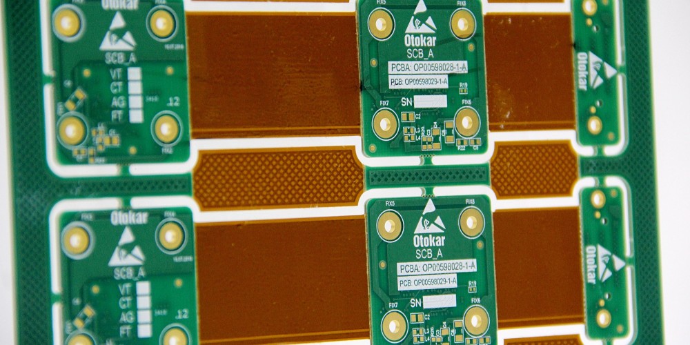
6 layer PCBs have 6 alternating layers of copper and substrate. They offer the following advantages compared to 2 or 4 layer boards:
- Higher component packing density: More routing layers allow tracks to pass both horizontally and vertically across the PCB layers. This enables fitting more components.
- Better electrical performance: Added layers reduce track lengths, minimize loops and allow better impedance control through matched track geometries. This improves signal quality and speed.
- Lower EMI: Ground planes between signals layers shield and isolate signals, reducing EMI noises. Multi-layer PCBs have better signal integrity.
- Heavier power handling: Power and ground planes distribute current smoothly reducing thermal stress and allowing heavier loads.
- Miniaturization: Greater complexity can be fit into a smaller PCB footprint area compared to fewer layers.
In summary, 6 layer rigid PCBs provide an optimal balance of complexity, performance and compactness for many mid-range applications.
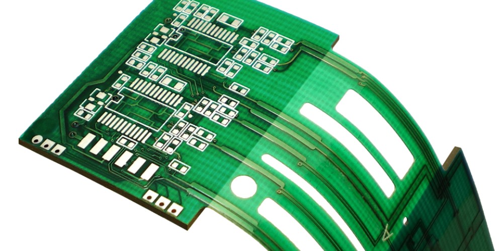
What is a Flex PCB?
Flex PCB use a flexible substrate like polyimide. They can bend and flex during use. Flex PCBs have from 1 to about 12 layers, with 2 to 6 being common.
Flex PCB properties:
- Can conform to any shape and be dynamically flexed. Enables innovative packaging and moving mechanisms.
- Extremely thin and lightweight. Complex circuity can be fit into tight spaces.
- Can be folded and assembled as 3D packages. Provides space efficiency.
- Tolerant of vibrations and moving parts with dynamic flexing. Suited for automotive and robotics use.
- Supports high density interconnects. Can replace bulky wiring harnesses.
Key applications of flex PCBs are in consumer electronics, computing and mobile devices. The flexible construction enables convenient packaging and portability.
Construction of 6 Layer Rigid and 2 Layer Flex PCBs
6 Layer Rigid PCB Stackup
A typical 6 layer rigid PCB stackup consists of:
- Top and bottom solder masks for insulation and markings.
- Top and bottom silkscreen layers for component information.
- 6 copper layers for signals and planes.
- 5 substrate cores separating copper layers.
- Plated through holes (PTHs) and vias for vertical interconnections.
The 6 copper layers are stacked as follows:
- Top: Signal layer
- L2: Ground plane
- L3: Signal layer
- L4: Power plane
- L5: Signal layer
- Bottom: Signal layer
The ground and power plane provide shielding between signals. The layer stackup is designed for controlled impedance signal routing.
2 Layer Flex PCB Construction
A 2 layer flex PCB contains:
- Bottom substrate layer of polyimide. Less flexible than 1 layer but cheaper.
- Bottom copper signal layer.
- Coverlay/solder mask as insulation coating over bottom layer.
- Top polyimide substrate layer. Thinner for maximum flexibility.
- Top copper signal layer.
- Coverlay/solder mask coating over top.
Vias and component pads are openings in the coverlay to expose copper. Flex PCBs use fewer vias due to flexing issues. Components mount only on one side.
Manufacturing Process
6 Layer Rigid PCB Fabrication
The generic PCB fabrication process is followed. Additional steps for 6 layers:
- Sheets of FR-4 substrate are laminated with copper foils on both sides to create 5 double-clad core boards.
- Cores have alignment holes drilled for layer-to-layer registration.
- Inner copper layers are individually coated with photoresist and then exposed to define the circuit pattern geometries.
- Exposed copper is etched away, while photoresist protects the tracks. This forms the inner circuit layers L2 to L5.
- Bookbinder machines are used to stack the cores and prepreg bonding sheets together under heat and pressure for curing. This fuses the boards into a 6 layer PCB sandwich.
- Alignment holes ensure inner layers are precisely stacked. Registration is critical.
- Outer conductor layers are added similarly by etching L1 and L6 outer copper layers of the stack.
- PTH drilling, plating, solder mask and silkscreen printing complete fabrication.
2 Layer Flex PCB Fabrication
Key steps are:
- Coverlay/solder mask is laminated onto bottom substrate layer.
- Bottom copper layer is etched to form conductor traces after photolithography.
- Top substrate layer is bonded. It is thinner than bottom for maximum flex.
- Top copper layer is added by etching.
- Coverlay is added to top copper layer for insulation.
- Via holes are drilled through and plated. Components are soldered.
- Outline routing separates individual PCBs from panel.
Flex PCBs require specialized machinery to handle thin, flexible boards during fabrication.
Applications
6 Layer Rigid PCB Applications
Typical applications of 6 layer rigid PCBs:
- Communications infrastructure – Routers, switches, base stations. High speed data handling and RF performance benefit from additional layers.
- Automotive electronics – Engine control units, infotainment systems. Mix of digital and analog signals plus noise isolation requires layer count headroom.
- Industrial automation – PLCs, motor drives, HMI interfaces. Demanding electrical environments leveraged by robust multilayer construction.
- Test and measurement equipment – Oscilloscopes, signal generators, logic analyzers. Precision analog and digital circuitry need multilayer stability.
- Aerospace and defense electronics – Avionics systems, guidance systems, radar arrays. High reliability in harsh operating conditions achieved.
In summary, applications requiring a balance of moderate complexity, electrical performance, ruggedness, reliability and compactness favor 6 layer rigid PCBs. The higher 8+ layer counts are used in more advanced systems.
2 Layer Flex PCB Applications
Given their unique properties, typical uses of 2 layer flex PCBs include:
- Wearable devices – activity trackers, smart watches, medical monitors. Enable comfortable fit on body contours.
- Portable consumer electronics – cellphones, cameras, display modules. Compact, space saving construction.
- Robotics – arms, joints, manipulators. Flexibility enables movement and motion.
- Automotive – door harnesses, seat heaters, mirrors. Replace bulky cabling, safer routing.
- Medical – imaging cameras, hearing aids, implants. Biocompatible and miniaturized.
- Defense – soldier systems, guidance controls, munitions. Ruggedize electronics.
- Aerospace – avionics, engine sensors, payload systems. Vibration resistance.
Flex PCBs are thus ideal wherever electronics need to flex, move dynamically, or assume arbitrary contours for best fit in tight spaces.
Pros and Cons of Each Technology
| 6 Layer Rigid PCB | 2 Layer Flex PCB |
|---|---|
| Pros: | Pros: |
| – Moderately High wiring density | – Can conform to any shape |
| – Good electrical performance | – Extremely thin and lightweight |
| – Effective EMI shielding | – Tolerates vibrations and flexing |
| – Good thermal dissipation | – High density interconnects |
| – Reliable construction | – Enables innovative, space saving packaging |
| – Low cost for complexity offered | – Compatible with rigid PCBs using rigid-flex |
| Cons: | Cons: |
| – More expensive than 2 or 4 layers | – Typically only 1 or 2 layer designs |
| – Cannot be flexed or bent dynamically | – Components can only be mounted on one side |
| – Not well suited for small, portable applications | – More prone to damage with repeated flexing |
| – Challenging to fabricate with high yields | – Requires specialized handling during fabrication |
Frequently Asked Questions
Q1. What are the typical substrate thicknesses in a 6 layer PCB?
A1. A typical 6 layer FR-4 PCB stackup uses:
- 0.8 to 1.6mm thick cores
- 0.1 to 0.2mm thick bonding prepreg sheets
Total thickness is usually 1.6mm to 3mm depending on substrate choice.
Q2. Can we use 6 layer PCB construction with flex substrates like polyimide?
A2. Yes, 6 layer flex PCBs are certainly possible for very demanding flexible applications. Polyimide substrates around 0.05mm thick would be used to create thin, multilayer flex circuit boards. However, they are complex to fabricate and cost will be very high.
Q3. What are the typical trace widths and spaces used on outer layers of these PCBs?
A3. For 6 layer rigid PCBs, typical outer layer trace widths and spaces are:
- Trace widths: 0.1mm to 0.25mm
- Trace spacing: 0.1mm to 0.2mm
2 layer flex PCBs commonly have:
- Trace widths: 0.1mm to 0.15mm
- Trace spacing: 0.075mm to 0.15mm
Q4. Can we have completely different circuit layers on the flex and rigid portions of a rigid-flex PCB?
A4. Yes, typically the circuit layers are optimized separately on rigid and flex portions of a rigid-flex design. Connectivity between sections is achieved by extending a few traces across the junction. So circuit layers can be designed with complete flexibility on either section.
Q5. What are the typical minimum bend radii for flex PCBs?
A5. Typical minimum bend radii are:
- Static bends: 3-5 times PCB thickness
- Dynamic flexing: 7-10 times PCB thickness
So a 0.2mm 2 layer flex PCB would have min bend radius around 2mm (static) and 3mm (dynamic). Tighter bends risk conductor cracking.