
-

How are PCBs populated?
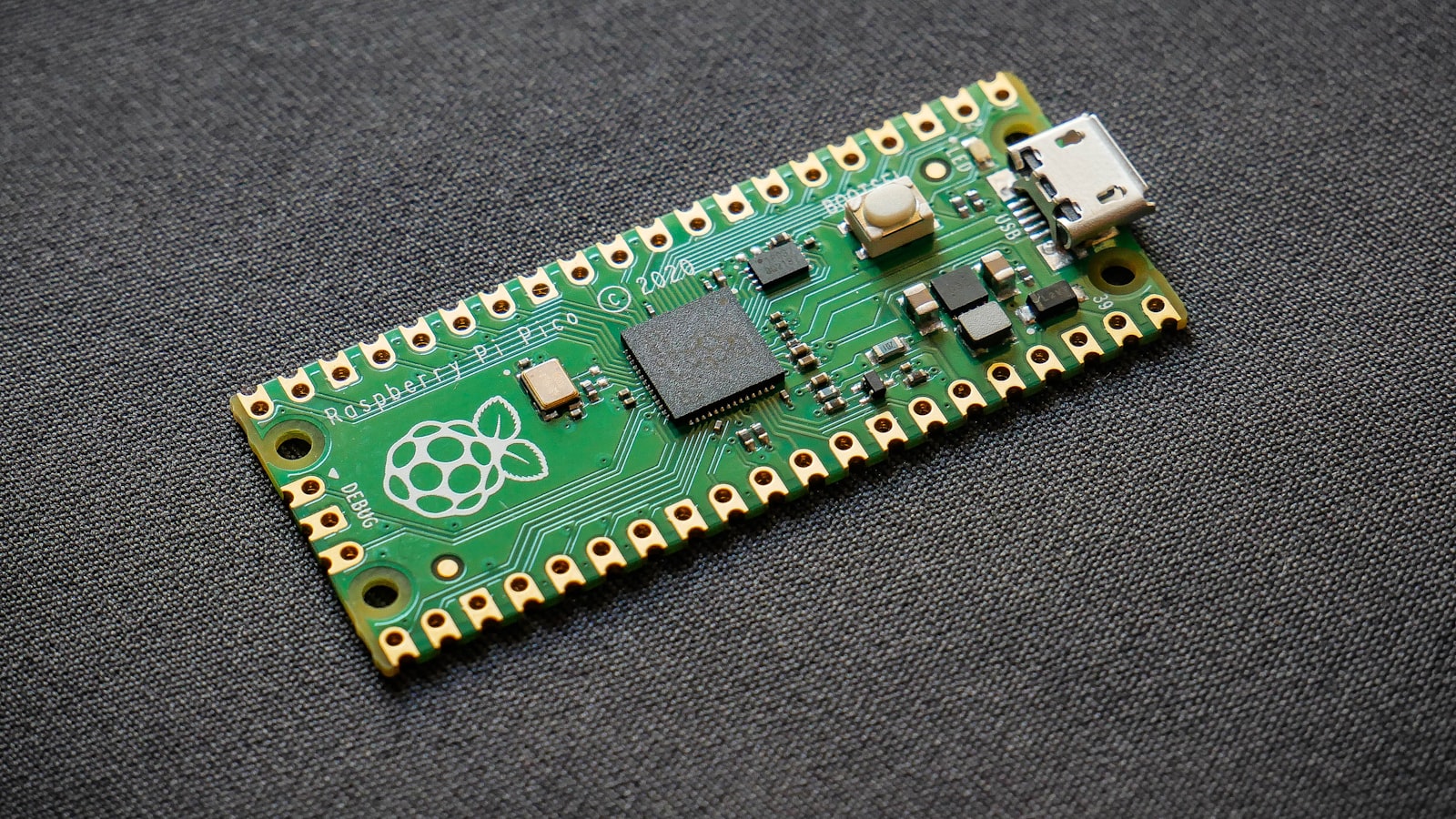
What is PCB population? PCB population, also known as PCB assembly or PCB stuffing, is the process of attaching electronic components to a printed circuit board (PCB). This process is crucial in the manufacturing of electronic devices, as it involves placing and soldering various components, such as resistors, capacitors, integrated circuits (ICs), and connectors, onto…
-
What is a stencil in PCB?
What is a PCB Stencil? A PCB stencil is a template used to apply solder paste onto the PCB pads during the surface mount assembly process. The stencil is placed on top of the PCB, and solder paste is spread across the stencil using a squeegee. The solder paste is deposited onto the pads through…
-

What is PCB stiffener?
Introduction to PCB Stiffeners A printed circuit board (PCB) stiffener, also known as a PCB stiffening bracket or PCB support, is a mechanical component used to provide additional rigidity and support to a PCB. PCB stiffeners are commonly used in applications where the PCB is subjected to vibration, shock, or other mechanical stresses that could…
-
What is Protel PCB?
Introduction to Protel PCB Protel PCB, also known as Altium Designer, is a powerful electronic design automation (EDA) software package used for designing printed circuit boards (PCBs). It is widely used by engineers, designers, and hobbyists to create high-quality PCBs for various applications, ranging from simple electronic projects to complex industrial systems. What is a…
-

What is a one layer PCB?
Introduction to Single Layer PCBs A printed circuit board (PCB) is the foundation of nearly all modern electronic devices. It provides mechanical support and electrical connectivity for electronic components using conductive pathways, tracks or signal traces etched from copper sheets laminated onto a non-conductive substrate. PCBs can be single sided (one copper layer), double sided…
-
How thick is gold on a PCB?
Understanding the Importance of Gold Thickness on PCBs When it comes to printed circuit boards (PCBs), the thickness of the gold plating plays a crucial role in determining the overall quality, durability, and performance of the board. Gold is a popular choice for PCB surface finishes due to its excellent conductivity, corrosion resistance, and ability…
-

What is a tombstone in PCB?
Introduction to Tombstoning in PCB Assembly Tombstoning, also known as the “Manhattan effect” or “Stonehenge effect,” is a common defect that occurs during the surface mount technology (SMT) assembly process of printed circuit boards (PCBs). This defect is characterized by the vertical standing of chip components, such as resistors or capacitors, on one end, resembling…
-

What is a two layer PCB?
Introduction to 2 Layer PCBs A two layer PCB, also known as a double-sided PCB or 2 layer printed circuit board, is a type of PCB that has conductive copper layers on both sides of the board substrate. The copper layers are used for interconnecting electronic components through conductive tracks, pads, and other features etched…
-
What is the process of PCB fabrication and assembly?
PCB Design and Preparation The PCB fabrication process begins with the design of the circuit board. This step involves creating a schematic diagram and a layout using specialized software such as Altium Designer, Eagle, or KiCad. The schematic diagram represents the electrical connections between components, while the layout determines the physical placement of components and…
-

What is the purpose of the annular ring in PCB?
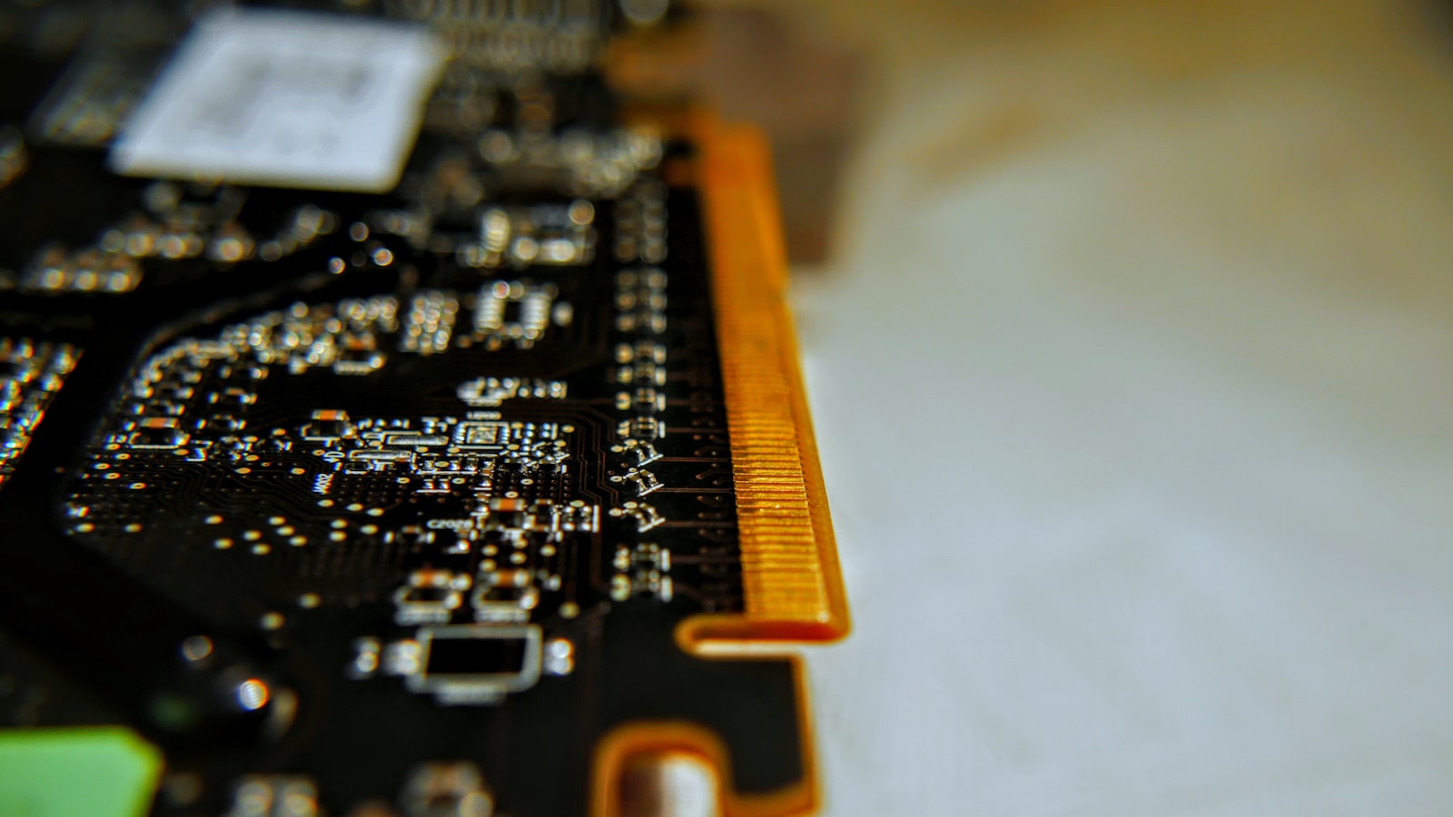
Introduction to Annular Rings in PCB Design In printed circuit board (PCB) design, an annular ring refers to the copper pad that surrounds a drilled hole or via. The annular ring serves several important purposes in PCB manufacturing and assembly. It provides mechanical support for component leads, allows for proper soldering, and ensures electrical connectivity…

March 2024
Archive
Categorise
Recent Posts
- Common Mode Choke Selection: A Comprehensive Guide
- Common Fab and Assembly Design Errors To Avoid – AltiumLive 2024
- Commodore 128 Principal Engineer, Bil Herd on Best Practices for Learning a New CAD Tool
- Collecting All the Pieces You Need: What is a Bill of Materials?
- Collaborative Design Software: Create PCB Schematic Symbols for any Component