


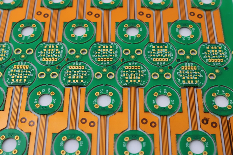
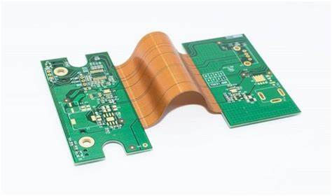
Rigid flexible printed circuit boards (PCBs), also known as flex circuits or flex PCBs, provide solutions for complex interconnections between components in electronic devices with space and weight constraints. Rigid flexible PCBs combine rigid FR-4 boards with flexible polyimide films bonded together in a single structure. The rigid sections provide mechanical support while the flexible sections allow dynamic flexing interconnections between components.
12 layer rigid flex PCBs offer more routing layers than traditional 2-8 layer boards for highly complex circuit designs. The additional layers enable higher component densities, miniaturization, and overall improved electrical performance. This article provides an overview of 12 layer rigid flexible PCB technology, design considerations, manufacturing processes, and applications across industries.
What are Rigid Flexible PCBs?
Rigid flexible PCBs integrate both rigid and flexible materials into a single circuit board solution. They contain:
- Rigid sections made of dielectric laminates like FR-4 for mechanical support
- Flexible sections made of polyimide films that allow dynamic movement
- Copper layers for traces and pads laminated between dielectric materials
The rigid and flex sections are bonded together with adhesive films. Components can mount on both rigid and flex areas. Conductive traces extend continuously between sections across flex-rigid transitions.
Rigid flex PCBs provide:
- Dynamic flexing interconnections
- Reduced weight and size
- Three-dimensional design freedom
- Enhanced reliability with fewer connectors
- Improved high frequency performance
Common applications include aerospace, medical, automotive, robotics, and consumer electronics.
12 Layer PCB Stackup Configurations
While 2-8 layer rigid boards are common, some applications require more complex 12+ layer stackups. Here are some typical 12 layer rigid flex stackup configurations:
12 Layer All Rigid
This stackup consists of 12 copper layers laminated between 13 dielectric layers. All layers are rigid FR-4 or other laminate material. The layers are bonded using prepreg resin.
12 Layer Rigid-Flex
This is a 12 layer rigid-flex stackup with 6 flexible layers and 6 rigid layers. The polyimide flex dielectric provides flexing zones between rigid regions. The layers are bonded with acrylic adhesive films.
12 Layer High Density Interconnect (HDI)
HDI PCBs use thinner dielectrics, tighter trace spacing, and microvias for high component density. This 12 layer HDI stackup has 4 buried vias and complex power/ground configurations. HDI allows increased routing in less space.
12 Layer Rigid Flex PCB Design Considerations
Designing a 12 layer rigid flex PCB requires advanced skills and engineering collaboration. Here are some key design considerations:
Layer Stackup
The designer must plan the layer stackup – the sequence of dielectric, copper, and adhesive layers. This defines the layout space and component placement. Important factors include:
- Number of layers: 12+ layers provide added routing but increase cost and complexity. Evaluate whether added layers are required.
- Dielectric materials: Choose rigid and flexible dielectrics suited for the application and environment. Consider thickness, flex and bend radii limits.
- Copper thickness: Thicker copper (2+ oz) has lower loss for high frequency or high current. Thinner copper saves space.
- High density interconnect (HDI) with buried vias is an option for ultra-dense packing.
- Ensure adequate ground/power layers for signal integrity.
Rigid-Flex Transition
The transition between rigid and flex sections impacts reliability. Follow guidelines for:
- Minimum rigid section lengths for component attachments
- Flex corner shapes (teardrop, rounded, swept arc)
- Annular ring width where copper traces cross from rigid to flex
- Coverlay overlap for stress relief at transitions
Component Placement
Optimize placement for routing, thermal management, and manufacturability:
- Place components on rigid sections for mounting stability
- Ensure clearance around taller components for flex bends
- Group high-speed components near rigid sections
- Symmetry for even layer usage and heat dissipation
Routing
With 12+ layers, manual routing is very difficult. Use autorouters intelligently:
- Set complete constraints for critical nets
- Autoroute non-critical nets
- Review and manually tune autorouter results
- Plan power and ground grids early
- Use wide traces for power handling
- Use vias/buried vias for layer transitions
Modeling and Analysis
Modeling and analysis helps verify the design:
- Thermal modeling to optimize heat sinks and airflow
- Vibration analysis on dynamic flex areas
- 3D EMI modeling for electrical performance
- Signal integrity simulations for high-speed signals
- DFM analysis for manufacturability
Collaborate with manufacturers and analysts early when planning layer stackups and component layout.
12 Layer Rigid Flexible PCB Manufacturing Process
Manufacturing complex 12+ layer rigid flex PCBs requires advanced processes, precision, and experience.
Layer Preparation
Each layer material must be prepared for lamination:
- Copper foils are electrodeposited onto rigid laminates and flex dielectrics
- Layers are cleaned and coated with oxide for adhesion promotion
- Photoimageable dry films are added for etching
Layer Alignment and Lamination
The layers are precisely aligned and laminated under heat and pressure:
- Layers are manually or optically aligned using tooling holes
- Multizone laminating presses apply programmable temps, pressures, vacuum, for adhesion
- Layers are fused into a monolithic PCB panel
Drilling
Lasers or mechanical drills create via holes through the bonded stackup:
- CNC mechanical drills with carbide and diamond bits drill holes down to 0.2mm size
- Laser drilling achieves microvias down to 0.05mm for HDI boards
- Depth is precisely controlled to avoid hitting buried layers
- Debris is removed from holes
Metallization
The walls of drilled holes are plated with copper to form the interlayer connections:
- Electroless copper coats the hole walls
- Electrolytic copper then deposits to desired thickness
- A chemical process ensures copper adhesion
Patterning
Etching with photoresists transfers the designed circuit pattern onto the layers:
- Dry film or liquid photoresist coats boards
- Ultraviolet light is exposed through the mask onto resist
- Exposed areas become soluble and unexposed areas remain on board
- Etchant solution removes unwanted copper
- Photoresist is stripped away
Solder Mask and Silkscreen
Solder mask insulates copper traces from solder. Silkscreen identifies components:
- Ultraviolet solder mask material coats the board
- Silkscreen epoxy ink is applied over solder mask
- Both are cured with UV exposure
Testing and Finishing
Completed boards are tested and finished:
- Automated optical inspection looks for defects
- Flying probe or bed-of-nails fixtures test connections
- Immersion silver protects exposed copper from oxidation
- Labels and protective coatings are added
This complex process flow requires quality control at each stage.
Applications of 12 Layer Rigid Flexible PCBs
12+ layer count rigid flex boards enable solutions in space-constrained and high performance products:
Aerospace and Defense
- Guided missiles – Interconnect guidance systems, thrust vector controls
- Unmanned aerial vehicles (UAVs) – Connect control and communications
- Avionics – Rugged boards for radar, controls, navigation
- Satellites – Rigid flex replaces wire harnesses, withstands vibration
Automotive Electronics
- Engine control units (ECUs) – Circuit density for engine monitoring
- Drive control modules – Flexible connections for steering/braking
- Advanced driver assistance systems (ADAS) – High speed boards for sensors
- Infotainment – Dynamic displays, rear view cameras
Medical Equipment
- Imaging systems – High resolution boards for X-ray, MRI, ultrasound
- Patient monitors – Flexible interconnects for ECG, blood oxygen sensors
- Surgical robots – Precision instrument control
- Implantables – Compact circuitry fits pacemakers, neurostimulators
Consumer Electronics
- Smart phones – Rigid flex connects displays, cameras, buttons
- Laptops – Interconnect motherboard and displays
- IoT devices – Compact, high density boards
- Wearables – Flexible boards conform to watches, fitness trackers
Frequently Asked Questions
Here are some common FAQs about 12 layer rigid flexible PCBs:
What are the key benefits of 12 layer rigid flex PCBs?
The main benefits are increased routing layers for complex circuits, integration of rigid and flexible sections, reduced weight/space demands, improved electrical performance, and dynamic interconnections.
When should 12 layers be used instead of 6 or 8 layers?
Use 12+ layers when a design requires routing density greater than 8 layers can provide, such as advanced microprocessors, FPGAs, RF designs, and high pin count components. The extra layers can also provide more power planes.
What are limitations of rigid flexible PCBs?
Limitations include higher fabrication costs, specialized design expertise needed, minimum bend radius restrictions on flex areas, and potential for flex cracking over time. Thermal management can also be a concern.
What types of analysis are recommended for 12 layer rigid flex designs?
Thermal analysis ensures components are within temperature limits. Vibration analysis verifies flex areas withstand dynamic stresses. Signal integrity analysis optimizes high speed signals. DFM analysis validates manufacturability.
How precise is layer alignment and registration for 12 layer boards?
Leading manufacturers specify registration accuracy around 25 microns (0.001″) or better for alignment of sequential layers. Laser drilling also achieves high precision on hole locations.
Conclusion
12 layer count rigid flexible PCBs provide advanced interconnect solutions for complex, dense circuit designs. The combination of rigid and flexible sections in one board enables superior electrical performance, three-dimensional shaping, dynamic flexing, and miniaturization. While design and fabrication are challenging, 12 layer rigid flex PCBs deliver capabilities beyond traditional boards. With rapid advances in electronic components, PCB technology continues to progress, making 12+ layer rigid flex PCBs accessible and beneficial across many industries moving forward.