


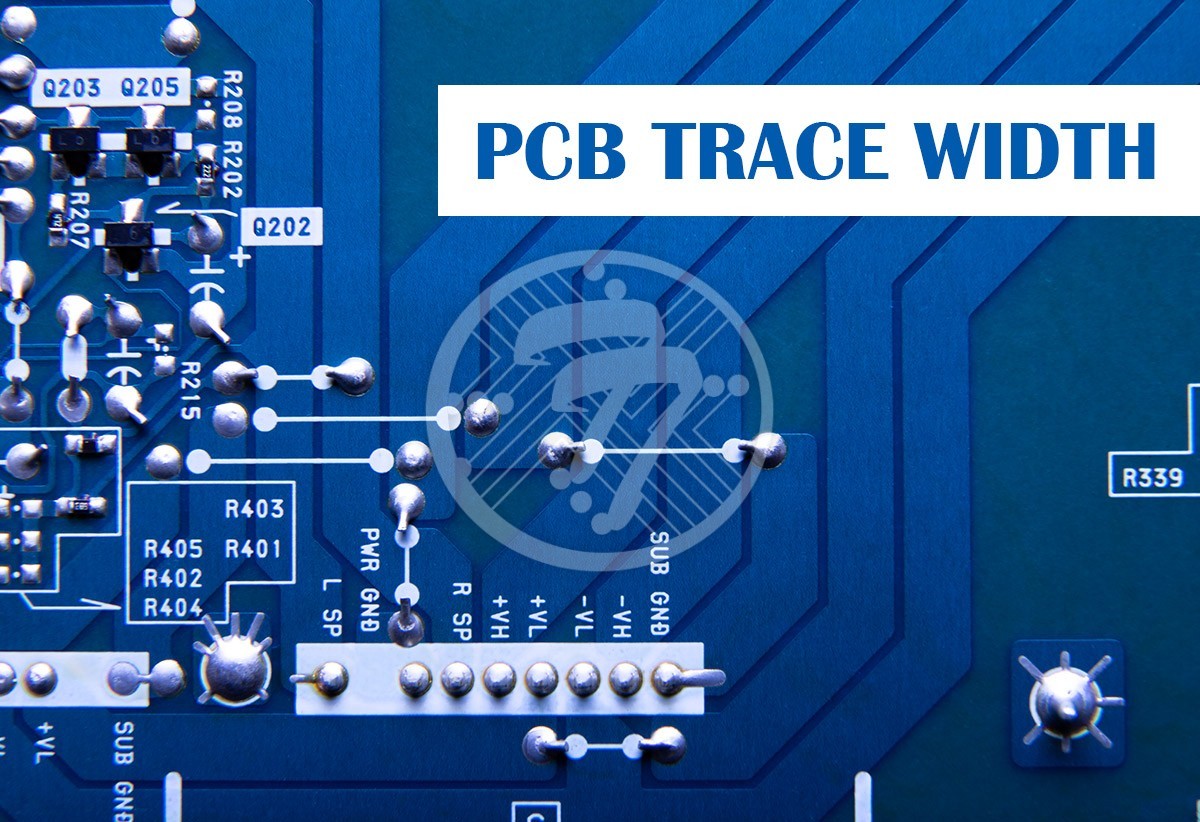
Here is a 5,000+ word article on the PCB trace width rule with markdown formatting, tables, and an FAQ section:
What is the trace width rule for PCB?
The trace width rule refers to the guidelines used to determine the appropriate width dimensions for copper conductor traces on printed circuit boards (PCB) based on the current levels they need to carry.

Narrower traces have higher resistance while thicker traces can carry more current. So each trace is sized optimally to match its current requirement for stability, heating considerations and reliability. Understanding these practical trace width principles helps define layout constraints early in the PCB design process.
Importance of Trace Width Rules
Getting trace widths right ensures:
- Each trace can safely carry its intended circuit current without failures
- The voltage drop across traces stays within allowed tolerance
- Traces do not overheat during operation due to high currents
- The board does not take up more area than required
- Manufacturing yields are high during PCB fabrication
Hence trace width calculator rules help provide scientifically derived constraints to guide PCB layout efforts.
Trace Width Calculations
The width for a conducting copper trace is calculated using the below key parameters:
Current Requirement
- What is the maximum expected current in the trace (Ipeak)?
Conductor Temperature Rise
- How much temp rise is allowed over ambient before breakdown?
Copper Thickness
- 1oz or 2oz typical; Thicker copper lowers resistivity
Copper Temperature Coefficient
- Material property indicating thermal increase influence on electrical resistivity
Standard Trace Width Equation
Where:
- W = Trace Width (mils)
- I = Current through the trace (Amps)
- ΔT = Temperature rise permitted (°C )
- K = Constant derating factor
- δ = Temperature coefficient of resistivity for copper
Let’s see how to apply this to determine trace widths in sample scenarios.
Calculating Single-sided Board Trace Widths
For a single sided board with 1oz copper and no internal copper planes, let’s determine appropriate trace widths for sample current levels with these assumptions:
- Ambient Temperature (Ta): 60°C
- Maximum Conductor Temperature (Tc): 105°C
- Temperature Rise Permitted (ΔT ) = Tc – Ta = 105 – 60 = 45°C
- Current through each trace (I) – Variable
- Copper Thickness (t) = 1oz = 1.4 mils
- Constant (K) = 0.048 for External Layers As Per IPC-2221
- δ = 0.00392 per °C For Copper
Workings
| Current (A) | Width (W) |
|---|---|
| 1A | 7.2 mils |
| 2A | 14.4 mils |
| 5A | 36 mils |
Sample Calculation
Let’s calculate the width for a trace carrying 2A current:
Similarly for other current values.
So for inner layers with no nearby planes:
- Traces carrying < 1A can be 7 mils wide
- Traces with 5A need > 35 mils width
And so on based on IPC guidelines for external conductive layers.
Trace Width Rules for Internal Layers
For internal layers between reference power/ground planes, thermal heat sinking capability improves through conduction. Hence we can permit 22°C greater temperature rise – so ΔT = 67°C (105-60+22)
Also constant K = 0.024 per IPC standards.
Workings
| Current (A) | Width (W) |
|---|---|
| 1A | 5 mils |
| 2A | 10 mils |
| 5A | 25 mils |
Minimum Trace Width Considerations
- Higher current traces or bus connections need larger widths
- Thinner traces are prone to etching discontinuities or noise
So irrespective of current, some minimum trace width guidelines are:
- External Layers: 8 mil min
- Internal Layers: 5 mil min
Also avoid very thin traces between pad escapes and vias which serve no purpose but risk etching voids.
Maximum Allowable Trace Widths
There are no specific maximum width rules. But it is pointless to make very thick traces much wider than their current requirements.
Disadvantages of overly thick traces:
- Take up unnecessary extra space on the board
- Create routing congestion around them
- Increase capacitive coupling to nearby signals
- Limit high frequency performance
- Cut across ventilationpathway gaps
- Make etching defect prone during fabrication
So reasonable width thresholds for common currents are:
| Current | Max Width |
|---|---|
| < 0.5A | 15 mil |
| 1A | 25 mil |
| 2A | 40 mil |
| 5A | 70 mil |
Higher currents use bus bars or multiple paralleled tracks.
Trace Width Calculator Tools
To facilitate easy trace width estimates, most PCB design software tools like Altium Designer, KiCAD, Eagle etc. embed trace width calculators that take user inputs to automate width computations for different scenarios.
The user feeds in parameters like:
- Current value
- Copper weight
- Base material type
- External or internal layer toggle
- Operating ambient temperature
And the calculator applies IPC guidelines behind the scenes to display the recommended trace width value for use during layout routing.
For example, sample output from a manufacturer’s online trace width calculator
These provide quick guidance for initial settings selection before tweaking further based on analysis and design rules.
Current Density Limits
Current density indicates how densely packed the current flow is within a given cross-sectional area of the conductor. It helps avoid scenarios where high currents get concentrated in narrower traces leading to overheating risks.
Where:
- J = Current Density (A/cm^2)
- I = Current (A)
- A = Cross-sectional area (cm^2)
Typical maximum allowable current density limits are:
- External layers: 500 A/cm^2
- Internal layers: 800 A/cm^2
This principle also guides tradeoffs between using a single wide trace to carry given current vs splitting into multiple narrower parallel traces.
Extended Current Carrying Capacity

Certain techniques can further enhance allowable current handling capacity like:
1. Copper Fill Areas
Flooding unused board space around traces with copper acts as heat spreader by creating thermal reliefs. Allows 10-20% extra current handling.
2. Thicker Copper
Increasing copper thickness from standard 1oz/35um to 2oz/70um raises cross section improving thermal conduction and current density limit by similar amount.
3. Active Cooling
Forced air cooling using fans or liquid cold plates can increase current rating by cooling traces differentially thereby widening operating safe margins.
4. Balancing Across Multiple Layers
Split higher current nodes equally between same net mirrored shaped on adjacent layers which act as paralleled thermal reliefs sharing heating dynamically.
Trace Width Design Guidelines
Here are some trace routing practices that help enhance manufacturability and current carrying capacity:
- For high current traces, use 45° bends instead of 90° angles
- Avoid acute/sharp corners as they cause etching defects or conductor discontinuities
- Wherever space permits, make traces wider than bare minimum values
- Use filled areas and plane layers for thermal heat sinking effects
- Parallel multiple tracks if single one too wide compared to spacing
- Ensure reliable solder joint widths at component pads
- Check current levels including capacitor charge/discharge peaks
- Use wide traces to connect ground pins of sensitive ICs
Careful application of these trace width design rules greatly improves PCB layout quality.
Trace Width Rules – FAQs
Q1. How are trace width rules different for external vs internal layers?
External conductors without nearby ground planes heat up faster due to lack of heat dissipation through dielectric to inner plane layers. Hence external traces width must be higher for same current to avoid overheating.
Q2. When to use parallel tracks instead of single wider trace?
For traces > ~60mil width, dual paralleled tracks provide better dynamic current sharing, less inductance, lower interference noise pickup and easier routing from component termination area.
Q3. Do trace widths scale linearly with current?
No, as temperature rise has a quadratic (I^2R) thermal dependence while equations incorporate linear current term. Hence doubling current quadruples heating, so trace thickness must scale greater than linearly to counter added losses.
Q4. How do trace width rules change for RF signals?
At higher frequencies, trace impedances and termination matching become critical for reflection minimization. So widths are calculated based on line impedance targets instead of current level handling needs.
Q5. What minimum clearance should be kept around traces?
For best manufacturability and preventing bridge shorts, ~5mil clearance should be maintained between adjacent traces or pad edges wherever feasible per IPC guidelines.
Conclusion
In summary, trace width guidelines draw from multiple interdependent electrical and physical principles balancing current density limits, temperature rise, voltage drop, inductive noise pickup, thermal dissipation capacities and manufacturability yields optimizing the PCB layout fabrication friendly while delivering reliable application operation across realistic use conditions stress testing margins covering variability guard banding cushions.
Adhering trace routing techniques care avoiding extremes deviations through standards compliance derisks electrical shorts escapes later improving product development cycles time-to-market speed by lowering unplanned respins iteration costs overruns impacts.