

What is a PCB?
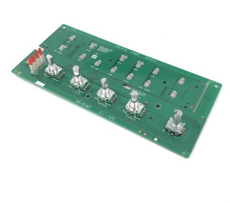
A PCB is a flat board made of insulating materials, such as fiberglass or composite epoxy, with conductive copper traces printed onto its surface. These traces connect various electronic components, such as resistors, capacitors, and integrated circuits (ICs), to form a complete electronic circuit. PCBs come in various sizes, shapes, and layers, depending on the complexity and requirements of the electronic device they are designed for.
Types of PCBs
PCBs can be classified into three main categories based on the number of layers they contain:
- Single-layer PCBs: These are the simplest and most cost-effective PCBs, consisting of a single insulating layer with conductive traces printed on one side only.
- Double-layer PCBs: These PCBs have conductive traces on both sides of the insulating layer, allowing for more complex circuits and higher component density.
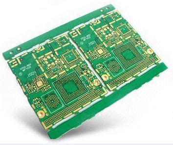
- Multi-layer PCBs: These are the most advanced and expensive PCBs, consisting of multiple insulating layers with conductive traces sandwiched between them. Multi-layer PCBs can have up to 50 layers or more, enabling highly complex and dense electronic circuits.
| PCB Type | Layers | Complexity | Cost |
|---|---|---|---|
| Single-layer | 1 | Low | Low |
| Double-layer | 2 | Medium | Medium |
| Multi-layer | 3+ | High | High |
Functions of PCBs
PCBs serve several critical functions in electronic devices, which can be broadly categorized into three main areas: mechanical support, electrical connectivity, and signal integrity.
Mechanical Support
One of the primary functions of a PCB is to provide mechanical support for the electronic components mounted on its surface. The PCB acts as a stable platform that holds the components in place, preventing them from moving or vibrating during operation. This is particularly important for devices that are subject to physical stress, such as smartphones, which can be dropped or bumped frequently.
The PCB’s mechanical strength is determined by several factors, including the type of insulating material used, the thickness of the board, and the number of layers. Thicker and multi-layer PCBs are generally more rigid and durable than thinner, single-layer boards.
Electrical Connectivity
The second primary function of a PCB is to provide electrical connectivity between the various components mounted on its surface. The conductive traces printed onto the PCB act as pathways for electric current to flow between the components, allowing them to communicate and function as a complete electronic circuit.
The layout and design of the conductive traces are critical to the PCB’s performance. The traces must be carefully routed to minimize signal interference, ensure proper grounding, and accommodate the power requirements of the components. The width and spacing of the traces also play a role in the PCB’s current-carrying capacity and signal integrity.
Signal Integrity
Signal integrity refers to the quality and fidelity of the electrical signals transmitted through the PCB. As electronic devices become faster and more complex, maintaining signal integrity becomes increasingly challenging. PCBs must be designed to minimize signal distortion, crosstalk, and electromagnetic interference (EMI) to ensure reliable and efficient operation of the electronic device.
Several techniques are used to improve signal integrity in PCBs, including:
- Controlled impedance: Designing the PCB traces to have a specific impedance value that matches the impedance of the components and connectors, reducing signal reflections and distortions.
- Differential signaling: Using pairs of traces with opposite polarity to transmit signals, canceling out electromagnetic interference and reducing crosstalk.
- Ground planes: Incorporating dedicated ground planes in the PCB to provide a low-impedance return path for signals, minimizing EMI and improving signal quality.
- Shielding: Using conductive materials, such as copper or aluminum, to shield sensitive traces and components from external EMI sources.
| Technique | Purpose | Benefit |
|---|---|---|
| Controlled impedance | Match trace impedance to components | Reduces signal reflections and distortions |
| Differential signaling | Cancel out EMI and crosstalk | Improves signal quality and reliability |
| Ground planes | Provide low-impedance return path | Minimizes EMI and improves signal quality |
| Shielding | Protect sensitive traces and components | Reduces external EMI interference |
PCB Manufacturing Process
The PCB manufacturing process involves several steps, each of which plays a critical role in the final quality and functionality of the board. The main steps in PCB manufacturing are:
- Design: The PCB design is created using specialized software, such as Altium Designer or Eagle. The design includes the component layout, trace routing, and any necessary mechanical features.
- Printing: The PCB design is printed onto a photosensitive film or directly onto the copper-clad insulating material using a plotter or laser printer.
- Etching: The printed PCB is exposed to ultraviolet light, which hardens the photosensitive film or copper-clad material. The unexposed areas are then chemically etched away, leaving the desired conductive traces.
- Drilling: Holes are drilled into the PCB to accommodate through-hole components and provide electrical connections between layers in multi-layer boards.
- Plating: The drilled holes are plated with conductive materials, such as copper or tin, to ensure reliable electrical connections.
- Solder mask and silkscreen: A protective solder mask is applied to the PCB to prevent accidental short circuits during soldering. A silkscreen layer is then added to provide component labels and other identifying marks.
- Surface finish: A final surface finish, such as HASL (Hot Air Solder Leveling) or ENIG (Electroless Nickel Immersion Gold), is applied to the PCB to protect the copper traces from oxidation and improve solderability.
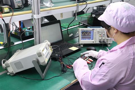
- Quality control: The finished PCB undergoes a series of quality control tests, including visual inspection, electrical continuity testing, and functional testing, to ensure it meets the required specifications.

Significance of PCBs in the Electronics Industry
PCBs have revolutionized the electronics industry by enabling the miniaturization, reliability, and mass production of electronic devices. Some of the key benefits of PCBs include:
- Miniaturization: PCBs allow for the compact and dense packaging of electronic components, enabling the creation of smaller, more portable devices.
- Reliability: The robust mechanical support and reliable electrical connections provided by PCBs ensure the long-term stability and performance of electronic devices.
- Cost-effectiveness: The standardized manufacturing process and the ability to mass-produce PCBs have significantly reduced the cost of electronic devices, making them more accessible to consumers.
- Flexibility: PCBs can be designed and customized to meet the specific requirements of virtually any electronic device, from simple consumer gadgets to complex industrial and aerospace systems.
As technology continues to advance, the demand for more sophisticated and high-performance PCBs will only increase. Emerging trends, such as the Internet of Things (IoT), 5G networks, and artificial intelligence (AI), will drive the development of new PCB materials, manufacturing techniques, and design methodologies to meet the evolving needs of the electronics industry.
FAQ
- What is the difference between a PCB and a circuit diagram?
A circuit diagram is a schematic representation of an electronic circuit, showing the components and their interconnections. A PCB, on the other hand, is the physical realization of the circuit diagram, providing a platform for the components to be mounted and connected. - Can PCBs be repaired if damaged?
In some cases, PCBs can be repaired if the damage is minor and localized, such as a broken trace or a lifted pad. However, more extensive damage, such as delamination or severe burning, may require the PCB to be replaced entirely. - What is the environmental impact of PCB manufacturing?
PCB manufacturing involves the use of chemicals and materials that can be harmful to the environment if not properly managed. However, the industry has made significant strides in adopting more eco-friendly practices, such as using lead-free solder and recycling waste materials. Many PCB manufacturers also adhere to strict environmental regulations and standards, such as RoHS (Restriction of Hazardous Substances) and WEEE (Waste Electrical and Electronic Equipment). - How long do PCBs typically last?
The lifespan of a PCB depends on several factors, including the quality of the materials used, the manufacturing process, and the operating environment. In general, well-designed and manufactured PCBs can last for several decades, especially if they are not subjected to extreme temperatures, humidity, or physical stress. - What is the future of PCB technology?
The future of PCB technology is driven by the increasing demand for faster, smaller, and more interconnected electronic devices. Some of the emerging trends in PCB technology include the use of advanced materials, such as graphene and carbon nanotubes, the adoption of 3D printing for rapid prototyping and customization, and the integration of embedded components and sensors for smart and connected devices. As the electronics industry continues to evolve, PCBs will remain a critical enabler of innovation and progress.
In conclusion, PCBs are the unsung heroes of the electronics industry, providing the essential functions of mechanical support, electrical connectivity, and signal integrity that enable the operation and performance of virtually all modern electronic devices. As technology continues to advance, the role of PCBs will only become more critical, driving innovation and shaping the future of the electronics landscape.