


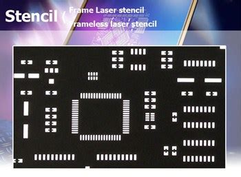
What Are PCB Stencils?
PCB stencils, also known as solder paste stencils, are thin metal sheets with precise apertures or openings that allow solder paste to be deposited onto specific areas of a printed circuit board (PCB) during the assembly process. These stencils play a crucial role in ensuring accurate and consistent solder paste application, which is essential for achieving reliable and high-quality solder joints.
Types of PCB Stencils
There are several types of PCB stencils available, each with its own unique characteristics and applications:
- Laser-Cut Stencils: These stencils are created using high-precision laser cutting technology, resulting in clean and accurate apertures. Laser-cut stencils are ideal for fine-pitch components and high-density PCB designs.
- Electroformed Stencils: Electroformed stencils are made by electroplating nickel onto a photoresist-patterned substrate. They offer excellent aperture accuracy and are suitable for applications requiring extremely fine features.
- Chemical-etched Stencils: Chemical-etched stencils are created by chemically etching the stencil material, typically stainless steel, to form the apertures. They are cost-effective and suitable for less demanding applications.
- Additive Stencils: Additive stencils are made by additively building up the stencil material, such as nickel, onto a substrate. They offer high accuracy and are suitable for complex and fine-pitch designs.
| Stencil Type | Aperture Accuracy | Cost | Suitable Applications |
|---|---|---|---|
| Laser-cut | High | Moderate | Fine-pitch, high-density designs |
| Electroformed | Excellent | High | Extremely fine features |
| Chemical-etched | Moderate | Low | Less demanding applications |
| Additive | High | High | Complex and fine-pitch designs |
The Role of Stencils in PCB Fabrication
Precise Solder Paste Deposition
One of the most critical roles of PCB stencils is to ensure precise solder paste deposition onto the PCB pads. The stencil apertures are carefully designed to match the size and shape of the PCB pads, allowing the right amount of solder paste to be deposited when the stencil is placed over the PCB and solder paste is applied using a squeegee.
Factors Affecting Solder Paste Deposition
Several factors can affect the accuracy and consistency of solder paste deposition:
- Stencil Thickness: The thickness of the stencil determines the volume of solder paste deposited. Thicker stencils deposit more solder paste, while thinner stencils deposit less.
- Aperture Size and Shape: The size and shape of the stencil apertures directly influence the amount and distribution of solder paste on the PCB pads. Apertures that are too small may result in insufficient solder paste, while oversized apertures may cause bridging or shorts.
- Stencil Material: The choice of stencil material can impact the release characteristics of the solder paste. Stainless steel is the most common material, offering good durability and paste release properties.
- Solder Paste Properties: The rheology (flow properties) and particle size of the solder paste also play a role in the deposition process. The solder paste must have the right consistency and flow characteristics to ensure proper release from the stencil apertures.
Preventing Solder Defects
Another important role of PCB stencils is to help prevent common solder defects that can occur during the assembly process. By controlling the amount and placement of solder paste, stencils can minimize issues such as:
- Solder Bridges: Solder bridges occur when excess solder paste connects adjacent pads, causing short circuits. Proper stencil aperture design and solder paste volume control can help prevent bridging.
- Solder Balls: Solder balls are small, spherical solder particles that can form on the PCB surface due to excessive solder paste or improper reflow conditions. Stencils with optimized aperture sizes and shapes can help reduce the occurrence of solder balls.
- Insufficient Solder Joints: Insufficient solder joints result from too little solder paste being deposited on the PCB pads. This can lead to weak or open connections. Stencils with appropriately sized apertures ensure that enough solder paste is deposited for reliable solder joints.
- Tombstoning: Tombstoning, also known as drawbridging, occurs when a component lifts up on one end during reflow, resulting in a tilted or vertical orientation. Stencils with balanced aperture designs can help prevent tombstoning by ensuring even solder paste distribution.
| Solder Defect | Cause | Prevention |
|---|---|---|
| Solder Bridges | Excess solder paste, adjacent pads | Proper aperture design, volume control |
| Solder Balls | Excessive solder paste, improper reflow | Optimized aperture sizes and shapes |
| Insufficient Joints | Too little solder paste deposited | Appropriately sized apertures |
| Tombstoning | Uneven solder paste distribution | Balanced aperture designs |
Enhancing Production Efficiency
PCB stencils also contribute to enhancing production efficiency in several ways:
- Faster Assembly: Stencils enable quick and consistent solder paste application, reducing the time required for manual or semi-automatic paste dispensing. This speeds up the overall assembly process.
- Improved Throughput: By ensuring precise solder paste deposition, stencils help minimize rework and repairs related to solder defects. This leads to higher first-pass yields and improved production throughput.
- Automated Compatibility: Stencils are compatible with automated solder paste printing equipment, enabling high-volume production and reducing the need for manual intervention.
- Scalability: Stencils can be easily scaled to accommodate different PCB sizes and designs, allowing for flexibility in production and the ability to handle a wide range of products.

Stencil Design Considerations
To achieve optimal results, several factors must be considered when designing PCB stencils:
Aperture Design
Aperture design is crucial for achieving the desired solder paste deposition. The size, shape, and pitch of the apertures should be carefully determined based on the PCB pad dimensions, component requirements, and solder paste characteristics. Proper aperture design ensures sufficient solder volume and prevents issues like bridging or insufficient solder joints.
Stencil Thickness
The thickness of the stencil directly affects the volume of solder paste deposited. Thicker stencils deposit more solder paste, while thinner stencils deposit less. The optimal stencil thickness depends on factors such as component pitch, pad size, and solder paste properties. Typically, stencil thicknesses range from 0.1 mm to 0.2 mm (4 to 8 mils) for standard SMT applications.
Escape Routing
Escape routing refers to the arrangement of traces and vias that connect the PCB pads to the rest of the circuit. Proper escape routing is essential for ensuring adequate space for stencil apertures and preventing solder paste contamination on adjacent pads or traces. The stencil design should take into account the escape routing strategy to optimize solder paste deposition and minimize potential defects.
Fiducial Marks
Fiducial marks are reference points on the PCB and stencil that help align the stencil with the PCB during the solder paste printing process. These marks are typically located at the corners or edges of the PCB and stencil. Accurate placement of fiducial marks ensures precise registration between the stencil and PCB, resulting in accurate solder paste deposition.
Stencil Material Selection
The choice of stencil material can impact the performance and durability of the stencil. Stainless steel is the most commonly used material due to its excellent durability, stability, and paste release properties. Other materials, such as nickel or polymer-based stencils, may be used for specific applications or to achieve finer aperture resolution.

Stencil Maintenance and Handling
Proper maintenance and handling of PCB stencils are essential for ensuring consistent performance and longevity. Some key considerations include:
- Cleaning: Regular cleaning of the stencil is necessary to remove solder paste residue and prevent contamination. Stencils can be cleaned using specialized stencil cleaning solutions or solvents in an ultrasonic cleaner.
- Storage: Stencils should be stored in a clean, dry environment to prevent damage or contamination. They should be kept in protective containers or bags when not in use.
- Handling: Stencils should be handled with care to avoid bending, warping, or damage to the apertures. Proper handling techniques, such as using gloves and supporting the stencil edges, can help maintain the integrity of the stencil.
- Inspection: Regular inspection of the stencil for signs of wear, damage, or contamination is important. Any issues should be addressed promptly to ensure consistent solder paste deposition and prevent defects.

Frequently Asked Questions (FAQ)
- What is the most common stencil thickness for SMT applications?
- The most common stencil thickness for standard SMT applications ranges from 0.1 mm to 0.2 mm (4 to 8 mils).
- How often should PCB stencils be cleaned?
- PCB stencils should be cleaned regularly, typically after every print cycle or as needed based on the solder paste type and printing volume. Regular cleaning helps prevent solder paste buildup and ensures consistent performance.
- Can damaged PCB stencils be repaired?
- In some cases, minor damage to PCB stencils can be repaired, such as smoothing out small dents or cleaning clogged apertures. However, if the damage is extensive or affects the aperture integrity, it is often more cost-effective to replace the stencil.
- What is the shelf life of a PCB stencil?
- The shelf life of a PCB stencil depends on various factors, such as the stencil material, storage conditions, and usage. With proper maintenance and handling, a stencil can last for several thousand print cycles. However, it is recommended to regularly inspect the stencil for signs of wear and replace it as needed.
- How do I choose the right stencil thickness for my PCB design?
- The choice of stencil thickness depends on factors such as component pitch, pad size, solder paste properties, and the desired solder joint profile. As a general guideline, a stencil thickness of 0.1 mm to 0.15 mm (4 to 6 mils) is suitable for fine-pitch components, while a thickness of 0.15 mm to 0.2 mm (6 to 8 mils) is appropriate for larger components. It is recommended to consult with your stencil manufacturer or assembly partner to determine the optimal stencil thickness for your specific PCB design.
Conclusion
PCB stencils play a vital role in the PCB fabrication process, ensuring precise and consistent solder paste deposition, preventing solder defects, and enhancing production efficiency. By carefully considering stencil design factors such as aperture size, stencil thickness, escape routing, and fiducial marks, manufacturers can optimize solder paste application and achieve high-quality solder joints.
Proper maintenance and handling of PCB stencils are equally important to ensure consistent performance and longevity. Regular cleaning, storage in a clean environment, careful handling, and inspection can help maintain the integrity of the stencils and minimize issues related to solder paste deposition.
As PCB designs continue to evolve with smaller components and higher densities, the importance of PCB stencils in the fabrication process will only continue to grow. By understanding the critical role of stencils and implementing best practices in stencil design and maintenance, manufacturers can ensure reliable and efficient PCB assembly, leading to high-quality electronic products.