


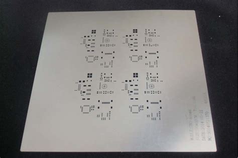
What is an SMT Stencil?
An SMT stencil is a flat sheet of metal, usually stainless steel or nickel, with laser-cut openings that correspond to the pads on a PCB. The stencil is placed on top of the PCB, and solder paste is applied using a squeegee. The solder paste is forced through the openings, depositing the right amount of paste onto the pads. The stencil is then removed, leaving the PCB ready for component placement.
Types of SMT Stencils
There are several types of SMT stencils, each with its own advantages and applications:
1. Stainless Steel Stencils
Stainless steel stencils are the most common type used in the industry. They offer excellent durability, precision, and are suitable for high-volume production. Stainless steel stencils come in various thicknesses, typically ranging from 0.1 mm to 0.2 mm (4-8 mils).
2. Nickel Stencils
Nickel stencils are an alternative to stainless steel stencils. They have a lower coefficient of thermal expansion, making them more stable in high-temperature environments. Nickel stencils are also more resistant to wear and tear, making them ideal for long production runs.
3. Polyimide Stencils
Polyimide stencils, also known as kapton stencils, are made from a flexible polymer material. They are often used for prototyping or low-volume production. Polyimide stencils are less durable than metal stencils but offer the advantage of being easily cut and modified.
4. Step Stencils
Step stencils are designed for PCBs with components of different heights. They have multiple levels or steps that accommodate the varying component heights, ensuring proper solder paste deposition on all pads.
5. Framed Stencils
Framed stencils are mounted on a metal frame, providing added stability and ease of handling. They are commonly used in high-volume production and automated assembly lines.
Importance of SMT Stencils
SMT stencils play a vital role in the SMT assembly process, contributing to the overall quality and efficiency of the final product.
1. Precise Solder Paste Deposition
One of the primary functions of an SMT stencil is to ensure precise solder paste deposition onto the pads. The laser-cut openings in the stencil are designed to match the size and location of the pads on the PCB. This precision ensures that the right amount of solder paste is applied, reducing the risk of insufficient or excessive solder, which can lead to defects such as bridging or tombstoning.
2. Consistent Solder Paste Volume
SMT stencils help maintain consistent solder paste volume across the entire PCB. The thickness of the stencil determines the amount of solder paste deposited on each pad. By using a stencil with the appropriate thickness, you can achieve uniform solder paste deposits, resulting in better soldering quality and fewer defects.
3. Increased Efficiency
Using an SMT stencil significantly increases the efficiency of the solder paste application process. Without a stencil, applying solder paste to individual pads would be a time-consuming and error-prone task. With a stencil, solder paste can be applied to all pads simultaneously, reducing the time and effort required.
4. Compatibility with Automated Assembly
SMT stencils are essential for automated assembly lines. They enable the use of solder paste printers, which can quickly and accurately apply solder paste to multiple PCBs in succession. This automation greatly increases production speed and consistency, making SMT stencils indispensable for high-volume manufacturing.

Stencil Design Considerations
When designing an SMT stencil, several factors must be taken into account to ensure optimal performance:
1. Aperture Size and Shape
The aperture size and shape of the stencil openings should match the size and shape of the pads on the PCB. The aperture size is typically slightly larger than the pad size to allow for some tolerance. The most common aperture shapes are rectangular and circular, but more complex shapes may be required for specific components or pad geometries.
2. Stencil Thickness
The thickness of the stencil determines the amount of solder paste deposited on the pads. Thicker stencils deposit more solder paste, while thinner stencils deposit less. The optimal stencil thickness depends on the size and pitch of the components, as well as the desired solder joint profile. Common stencil thicknesses range from 0.1 mm to 0.2 mm (4-8 mils).
3. Aperture Walls
The walls of the stencil apertures should be smooth and tapered to facilitate the release of the solder paste. Tapered walls help prevent solder paste from sticking to the stencil, ensuring clean and consistent deposits. The wall angle is typically between 5 and 7 degrees.
4. Fiducial Marks
Fiducial marks are reference points on the stencil that help align it with the PCB. They ensure accurate positioning of the stencil and prevent misalignment, which can lead to solder paste being deposited in the wrong locations. Fiducial marks should be strategically placed on the stencil and PCB to allow for easy alignment.

Stencil Maintenance and Cleaning
To ensure consistent performance and longevity, SMT stencils require regular maintenance and cleaning.
1. Cleaning Frequency
Stencils should be cleaned after every use or at regular intervals, depending on the production volume and the type of solder paste used. Cleaning helps remove solder paste residue, flux, and other contaminants that can affect the quality of the solder paste deposits.
2. Cleaning Methods
There are several methods for cleaning SMT stencils:
- Manual cleaning: Using solvents and wiping the stencil with a lint-free cloth.
- Ultrasonic cleaning: Immersing the stencil in an ultrasonic cleaner with a suitable cleaning solution.
- Automated cleaning: Using specialized stencil cleaning machines that combine solvent spray and wiping actions.
The choice of cleaning method depends on the type of stencil, the solder paste used, and the available resources.
3. Storage
When not in use, SMT stencils should be stored in a clean, dry environment to prevent contamination and damage. Stencils should be stored flat or hung vertically to avoid warping or deformation. Proper storage helps extend the life of the stencil and ensures its readiness for the next use.

FAQ
1. How often should I replace my SMT stencil?
The lifespan of an SMT stencil depends on several factors, such as the type of stencil, the frequency of use, and the cleaning and maintenance practices. On average, a well-maintained stencil can last for several thousand prints. However, it’s essential to regularly inspect the stencil for signs of wear, damage, or contamination. If the stencil shows signs of deterioration or if the print quality begins to suffer, it may be time to replace it.
2. Can I use the same stencil for different PCBs?
In general, each PCB design requires its own specific stencil. The stencil apertures are designed to match the pad size and layout of a particular PCB. Using the same stencil for different PCBs may result in incorrect solder paste deposition, leading to defects and quality issues. However, if multiple PCBs share the same pad layout, it may be possible to use a single stencil for those specific designs.
3. What is the difference between a laser-cut and a chemically etched stencil?
Laser-Cut Stencils are created using a high-precision laser to cut the apertures into the stencil material. This process allows for very fine pitch apertures and intricate designs. Chemically etched stencils, on the other hand, are made by selectively removing material using a chemical etching process. Chemically etched stencils are generally less precise than laser-cut stencils and are better suited for larger pitch components and less complex designs.
4. How do I choose the right stencil thickness?
The choice of stencil thickness depends on several factors, including the size and pitch of the components, the desired solder joint profile, and the viscosity of the solder paste. As a general rule, thinner stencils (0.1 mm to 0.15 mm) are used for smaller components and fine-pitch devices, while thicker stencils (0.15 mm to 0.2 mm) are used for larger components and higher-volume solder joints. It’s essential to consult with your stencil manufacturer or assembly service provider to determine the optimal stencil thickness for your specific application.
5. Can I reuse a cleaned SMT stencil?
Yes, a properly cleaned SMT stencil can be reused multiple times. However, it’s crucial to ensure that the stencil is thoroughly cleaned and free of any residue or contamination before reuse. Improper cleaning can lead to solder paste deposit inconsistencies and defects in subsequent prints. It’s also important to inspect the stencil for any signs of damage or wear before reuse, as a damaged stencil can negatively impact print quality.
Conclusion
SMT stencils are a critical component in the surface mount technology assembly process. They ensure precise, consistent solder paste deposition, increase efficiency, and enable automated assembly. By understanding the types of stencils, their design considerations, and proper maintenance and cleaning practices, you can optimize your SMT assembly process and achieve high-quality results.
Investing in a well-designed and well-maintained SMT stencil is essential for any electronics manufacturing operation. It can help reduce defects, increase yields, and ultimately lead to more reliable and cost-effective products.
| Stencil Type | Material | Thickness | Application |
|---|---|---|---|
| Stainless Steel | Stainless Steel | 0.1 – 0.2 mm | High-volume production |
| Nickel | Nickel | 0.1 – 0.2 mm | High-temperature environments |
| Polyimide | Polyimide (Kapton) | 0.05 – 0.13 mm | Prototyping, low-volume production |
| Step | Stainless Steel, Nickel | Varies | PCBs with components of different heights |
| Framed | Stainless Steel, Nickel | 0.1 – 0.2 mm | High-volume production, automated assembly |
| Stencil Thickness | Application |
|---|---|
| 0.1 – 0.15 mm | Smaller components, fine-pitch devices |
| 0.15 – 0.2 mm | Larger components, higher-volume solder joints |
By selecting the appropriate SMT stencil for your PCB design and assembly requirements, you can ensure optimal solder paste deposition and achieve the best possible results in your SMT assembly process.