


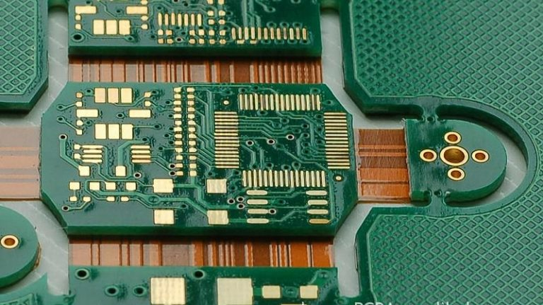
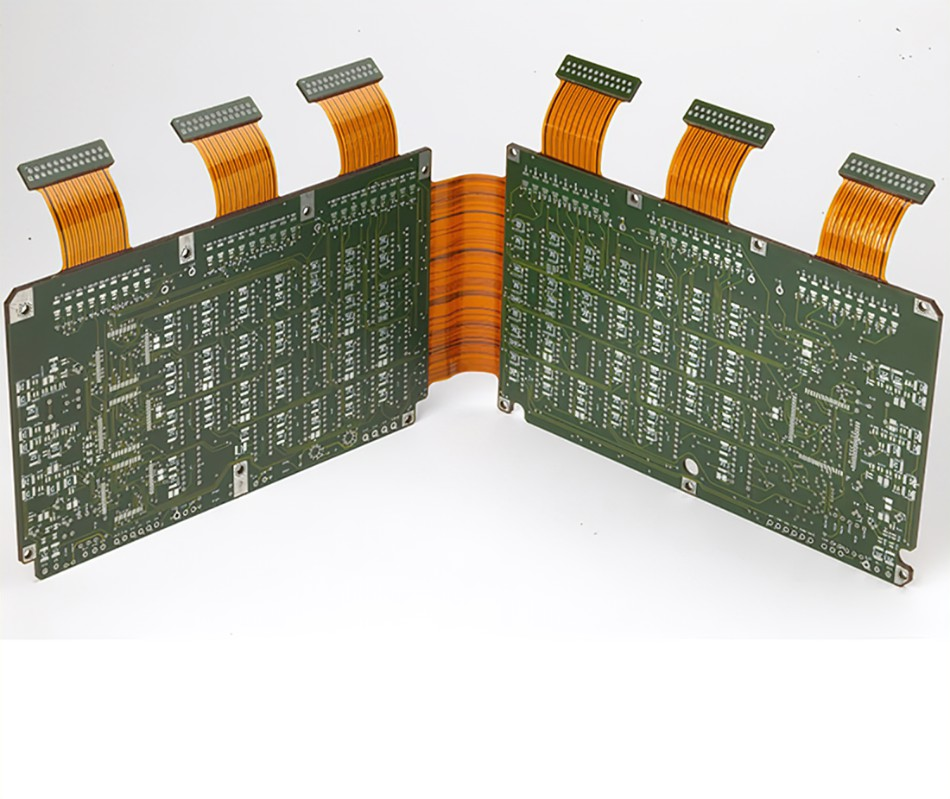
Rigid-flex PCBs, also known as rigid-flexible printed circuit boards, are circuit boards that consist of rigid and flexible substrates laminated together. They provide solutions for applications that require dynamic flexing, bending or folding while maintaining circuit integrity. The combination of rigid and flexible materials in one PCB allows for greater efficiency and improved reliability in electronic devices.
The manufacturing process of rigid-flex PCBs is more complex than that of regular rigid PCBs. It requires specialized materials and techniques to integrate the rigid and flexible layers together. This article provides an overview of the step-by-step rigid-flex PCB fabrication process.
Steps in Rigid Flex PCB Manufacturing Process
The main steps involved in manufacturing rigid-flex PCBs are:
1. Design and Layout
The first step is designing the PCB layout according to the required application. Rigid-flex PCBs require advanced design to integrate the rigid and flex layers properly. Some key considerations include:
- Determining the number of layers (rigid and flex) needed
- Identifying placement of components on rigid vs. flex areas
- Minimizing the number of flex-to-rigid transitions
- Maintaining appropriate spacing around bends and folds
- Accounting for differences in coefficients of thermal expansion (CTE)
- Incorporating necessary stiffeners and covers
Proper design is crucial for avoiding failures and ensuring optimal performance. Simulation and analysis tools are often used to validate the design.
2. Material Selection
Rigid-flex PCBs use a combination of rigid and flexible substrate materials that are bonded together. Common options include:
Rigid substrates: FR-4, polyimide, aluminum, copper
Flexible substrates: polyimide, polyester, copper-invar-copper
The materials are chosen based on factors such as dielectric properties, thermal capabilities, bend radius, cost, and compatibility. The coefficient of thermal expansion between materials must be matched to avoid separation or warping during temperature changes.
3. Imaging and Etching
The fabrication process begins with rigid and flex core layers. Laminated sheets of the substrate materials are coated with copper foil on one or both sides. Photoresist is then applied to transfer the circuit pattern onto the copper layers through a process of imaging and etching.
Imaging: The photoresist is exposed to UV light through a mask that contains the circuit pattern. This chemically changes the exposed areas of the photoresist.
Etching: The PCB panel is immersed in an etching solution to dissolve away unwanted copper that is unprotected by photoresist. This leaves behind the desired circuit pattern.
4. Layer Lamination
Multiple rigid and flex core layers are stacked together and aligned. Prepreg bonding sheets are inserted in between the layers. The layer stack then goes through a lamination press that applies heat and pressure. This bonds the layers together to form a unified board.
The number of layers depends on the complexity and density of interconnections required. High-layer-count PCBs (>12 layers) often use laser drilling for creating interlayer vias instead of mechanical drilling.
5. Drilling
The laminated board now undergoes drilling to create holes that connect different layers. In mechanical drilling, high-speed drill bits penetrate the stack to form vertical conduits for components and interlayer connections. The holes are then metallized with an electroplating process.
In laser drilling, focused CO2 laser beams ablate material to form microvias. This achieves higher precision drilling and works better for multilayer boards.
6. Bending and Stiffening
The flex areas of the PCB are then bent and folded into the required form. Ridged plates or frames called stiffeners are added to reinforce the rigid sections. Components are soldered onto the board before or after bending depending on design.
7. Final Testing and Finishing
The finished rigid-flex boards go through electrical and functional testing. Automated optical inspection (AOI) checks for any flaws. The boards are then routed into individual PCBs if required. Final finishing steps include cleaning, applying solder mask and protective coatings, and electrical testing.
Key Considerations
Some important considerations for rigid-flex PCB manufacturing include:
- The process requires advanced skills, expertise, and specialized equipment. Not all suppliers provide rigid-flex solutions.
- Materials must be carefully selected to withstand heating and bending stresses.
- Stack-up design is critical for reliability. It may require extensive modeling and analysis.
- Close tolerances are needed for drilling, cutting, and bending to avoid damage.
- More manual processes may be involved like layer alignment and stiffener placement.
- QA and testing is extensive given the risks of defects.
Benefits and Applications
The benefits of using rigid-flex PCBs include:
- Allows 3-dimensional shaping and dynamic flexing for ergonomic and space-saving product designs.
- Facilitates complex interconnectivity between multiple rigid PCBs assemblies. Replaces connectors and wires.
- Withstands mechanical stress and repetitive bending. Provides good vibration/shock resistance.
- Allows high component density and miniaturization. Good for portable and wearable products.
- Improves reliability and product life compared to flex-to-rigid connectors which are prone to failure.
Rigid-flex PCBs are used in a wide range of applications:
- Mobile phones, laptops, tablets
- Automotive camera systems and dashboard displays
- Aerospace and military systems
- Medical devices
- Consumer electronics
- Industrial robots and machinery
The rigid-flex fabrication process enables innovative designs not possible with rigid PCBs alone. With the right design and manufacturing approach, rigid-flex PCBs provide greatly enhanced reliability in demanding mechanical and electronic applications.
Frequently Asked Questions
Here are some common questions about rigid flex PCB manufacturing:
Q1. What are the minimum and maximum number of layers in rigid flex PCBs?
The minimum number of layers is 4 – 2 rigid outer layers and 2 inner flex layers. There is no specific maximum, but high-layer-count boards above 12 layers are uncommon and require advanced manufacturing capabilities. Most rigid-flex PCBs have between 4-8 layers.
Q2. What types of materials are used for rigid layers in rigid flex PCBs?
The most common rigid substrate is FR-4, which is a glass-reinforced epoxy laminate material. Other options include polyimide, PTFE composites, aluminum, and steel for very high stiffness requirements.
Q3. What is the smallest bend radius achievable with flex layers in rigid flex PCBs?
The bend radius depends on the flexible material used. Typical flex materials like polyimide and polyester can achieve bend radii down to 3-5mm. With special flex materials, the bend radius can be as low as 1mm.
Q4. What are some failure modes in rigid flex PCBs?
Potential failure modes include flex cracks, layer delamination, brittle fracture of conductors, and stress cracks in components mounted across flex areas. These are minimized through proper design, material selection, process control, and QA testing.
Q5. What types of tests are performed on rigid flex PCBs?
Testing involves electrical checks, continuity/connectivity testing, automated optical inspection, x-ray inspection of layer alignment, bend cycle testing for reliability, vibration/shock testing, and environmental stress testing like thermal cycling and humidity exposure.
Conclusion
Rigid-flex PCB technology enables flexible, three-dimensional circuitry design needed in many modern electronics. With both rigid and flexible materials integrated in one board, it provides mechanical stability as well as dynamic movement capabilities. Rigid-flex PCB fabrication requires meticulous process control and expertise across design, materials, stack-up, drilling, bending, and testing. When implemented correctly, rigid-flex PCBs offer greatly enhanced reliability and product performance over traditional rigid boards for today’s complex electronics.