


What is PCB Panelization?
PCB panelization is the process of combining multiple printed circuit board designs onto a single panel for manufacturing. By grouping boards together on a larger panel, it allows for more efficient fabrication since multiple boards can be produced in a single run.
The advantages of panelizing PCBs include:
- Reduced manufacturing time and cost per board
- Easier handling of smaller boards
- Optimized material usage with less waste
- Facilitates automated assembly when boards are panelized properly
At Screaming Circuits, we have extensive experience with PCB panelization to streamline the fabrication and assembly of our customers’ designs. Our expertise ensures high quality boards are manufactured and assembled as efficiently as possible.
PCB Panelization Techniques
There are several common PCB panelization techniques that can be used depending on the size, shape, and quantity of the boards being produced. The three main approaches are through-hole tab routing, v-scoring, and mousebites.
Through-hole Tab Routing Panelization
With through-hole tab routing, each individual board is connected to the main panel by small tabs. After the PCBs are fabricated and assembled, the tabs are cut or routed to separate the individual boards from the panel.
This method works well for most board shapes and sizes. The tabs are typically located on the outer edges of each board and are removed after depaneling. Proper placement of the routing tabs is critical to avoid damaging components near the board edges during depaneling.
V-score Panelization
V-scoring is a technique where a v-shaped groove is scored between each board on the panel. The individual PCBs remain connected to the main panel but can be easily separated by breaking along the v-score lines after assembly.
V-scoring allows the boards to be placed closer together on the panel compared to tab routing. This helps maximize the panel area and number of boards that can be produced. The clean, straight edges left behind after breaking the v-score also eliminates the need for secondary routing.
However, v-scoring does have several drawbacks and limitations:
- It only works for simple rectangular or circular boards
- Boards must have sufficient space along the edges for the v-score
- Not suitable for thicker PCBs over 1.6mm
- Components must be kept back from v-score lines to avoid damage during depaneling
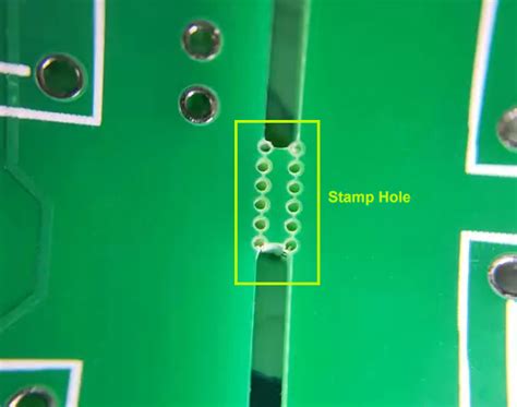
Mousebite Panelization
Mousebites, also known as breakaways or snap-offs, are a series of small holes drilled between PCBs on the panel. The boards are held together by the web of material between these perforations. After assembly, the individual boards can be snapped out of the panel by breaking along the mousebite holes.
Mousebites are the simplest and lowest cost panelization option. They work well for basic rectangular boards but are not suitable for more complex board shapes. There are also limitations on how close components can be placed near the edges to avoid interfering with the mousebites.

Guidelines for Designing Panelized PCBs
When designing PCBs that will be panelized, there are several guidelines that should be followed to ensure the best results:
Board Spacing
Sufficient space must be left between individual boards on the panel for the panelization method being used. The minimum spacing between boards depends on the board thickness and panelization technique:
| Board Thickness | Tab Routing | V-score | Mousebites |
|---|---|---|---|
| <0.8mm | 3mm | 1mm | 3mm |
| 0.8-1.6mm | 5mm | 2mm | 4mm |
| >1.6mm | 7mm | Not Recommended | Not Recommended |
Component clearance
Proper component clearance must be maintained from the edges of the individual boards to avoid damage during depaneling. At a minimum, components should be kept back at least 3mm from tab routed or v-scored edges. For mousebites, a minimum of 5mm component clearance is recommended.
Panelization Fiducials
Fiducial marks should be included on the main panel to facilitate proper registration and alignment during the assembly process. A minimum of three globally unique fiducials are required, preferably placed around the perimeter of the panel.
Locally unique fiducials for each board are also recommended, especially for smaller PCBs or those with fine pitch components. These local fiducials allow for more precise placement of components on the individual boards.
Tooling Holes and Rails
Tooling holes are used to align and secure the panel during fabrication and assembly. These holes should be placed in the main panel frame and not interfere with any of the individual board designs. The standard tooling hole size is 3.2mm diameter.
Tooling rails, or handling strips, around the edges of the panel provide extra rigidity and allow for easier handling of the panel. The width of the rail depends on the size and weight of the panel but is typically between 5-10mm.

Screaming Circuits Capabilities
At Screaming Circuits, we have the in-house expertise and capabilities to panelize a wide range of PCB designs. Our engineers work closely with customers to determine the best panelization approach based on their specific needs and requirements.
We support the following panelization options:
- Tab routing (up to 1.6mm thick boards)
- V-scoring (up to 1.2mm thick)
- Mousebites
For tab routing, we use either a pizza-cutter style or drill & route method depending on the board thickness and panel layout. Our v-score capabilities include both single and double-sided scoring for clean, easy depaneling.
Our automated assembly lines are optimized for panelized PCBs to provide fast, reliable placement of components. We can place components as close as 3mm from the edge of tab routed boards and 1mm from v-score lines.

Conclusion
PCB panelization is an important consideration for anyone looking to efficiently prototype or mass produce circuit boards. By combining multiple PCBs onto a single panel, you can save time and money on fabrication and assembly.
At Screaming Circuits, we have the knowledge and expertise to help guide you through the panelization process. Our team can assist with everything from panel layout and design to final assembly and testing.
If you have any questions about PCB panelization or our capabilities, please don’t hesitate to reach out. We’re here to help bring your circuit board designs to life!
Frequently Asked Questions
What is the maximum panel size you can support?
Our standard panel sizes range from 4″ x 4″ up to 16″ x 22″, but we can also accommodate custom panel sizes up to 22″ x 26″ if needed. The maximum panel size depends on the fabrication requirements and assembly equipment being used.
How much does panelization add to the cost?
The cost impact of panelization depends on the complexity of the panel layout and the fabrication/assembly processes required. In general, simple tab-routed designs will be less expensive than v-scored or complex mousebite layouts.
We work with our customers to find the most cost-effective panelization solution while still meeting their technical requirements. The overall savings from increased manufacturing efficiency can often offset the added cost of panelization.
What files do I need to provide for panelization?
For us to panelize your design, we will need the individual board Gerber files as well as an overall panel drawing or layout showing the desired arrangement of the boards on the panel. Additional fabrication and assembly files such as the drill drawing, netlist, and BOM may also be required depending on the project.
Our team can work with you to ensure all necessary files are provided and review your panel design before starting production.
How long does the panelization process take?
The panelization process typically adds 1-2 days to the overall fabrication and assembly cycle time. However, this can vary depending on the complexity of the panel layout and the specific requirements of the project.
We always aim to minimize any additional time required for panelization while still ensuring the highest quality results. If you have specific timelines that need to be met, please let us know so we can prioritize your project appropriately.
Can you panelize boards with different thicknesses?
In general, it is best to panelize boards that are the same thickness to ensure consistent fabrication and assembly processes. Mixing different board thicknesses on the same panel can lead to issues with warpage, uneven solder joints, and other manufacturing defects.
If you do need to panelize boards of different thicknesses, we recommend keeping the thickness variation to a minimum and using a rigid frame or substrate to support the thinner boards. Our team can advise on the best approach for your specific design.