


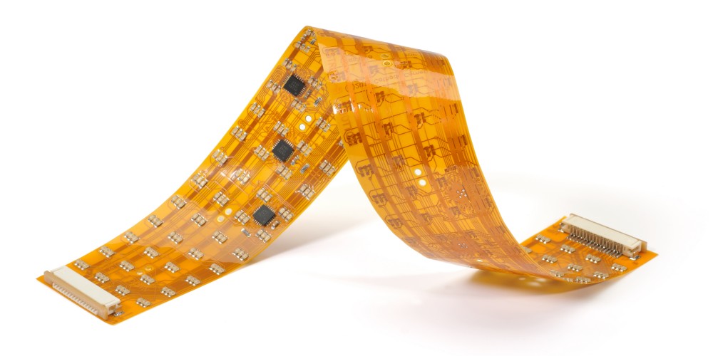
Introduction to Flex Rigid PCBs
Flex rigid printed circuit boards (PCBs) combine rigid and flexible circuitry into a single PCB assembly. They provide the ability to interconnect multiple rigid sections through flexible connections, allowing the board to flex and bend. This enables more compact and unique PCB form factors.
Some key benefits of flex rigid PCBs:
- Space savings – Flexible connections take up less space than traditional connectors.
- Weight reduction – Thinner flexible sections reduce overall weight.
- Improved reliability – Reduced connections points lower failure rates.
- Dynamic flexing – Allows movement between rigid sections.
- Design flexibility – More options for packaging and layout.
Flex rigid PCBs are commonly used in aerospace, medical, consumer electronics, industrial equipment and automotive designs. As electronics become more compact, designers are turning to flex rigid PCBs to fit more functionality into smaller products.
When to Use Flex Rigid PCBs
Flex rigid PCBs should be considered when:
- There is a need to interconnect multiple rigid PCBs.
- PCB space constraints exist and flexible connections can reduce space between sections.
- The design requires dynamic flexing between sections of the circuitry.
- Vibration, shock or repeated movement is a factor.
- Weight and/or volume reduction are important.
- Unique PCB shapes or form factors are required.
Key Design Considerations for Flex Rigid PCBs
Designing flex rigid PCBs requires specialized design tools and an understanding of the unique requirements. Here are some of the key considerations:
Layer Stackup
The rigid sections of the PCB will typically contain multiple copper layers (e.g. 4 to 28+ layers) while the flex sections are usually single or double layer. Adding more copper layers provides increased routing capacity but also increases thickness and cost.
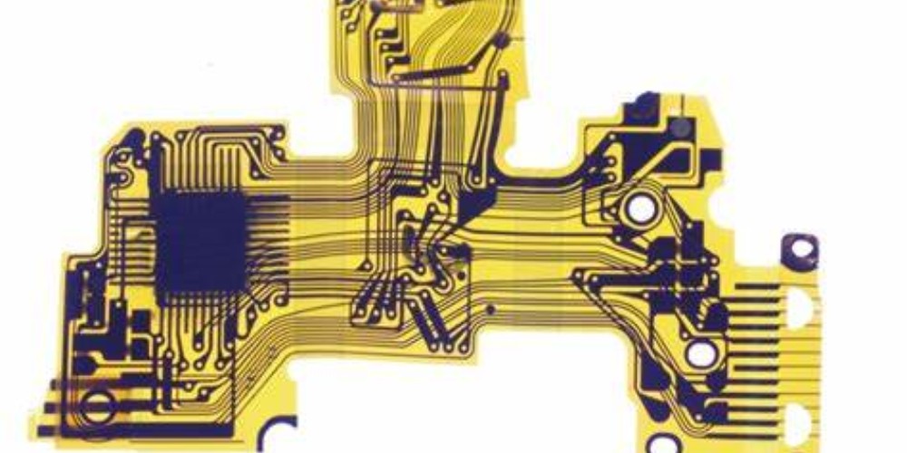
Flex Circuit Layout
Traces should be designed on the neutral axis to minimize stress and prevent traces from cracking. A minimum bend radius must be maintained to prevent damage to traces. Stiffeners and covers can be added for protection and support.
Rigid-Flex Transition
Special care must be taken where the rigid and flex sections interconnect. The board should be reinforced with solder mask or covers. Floating sections can help relieve stress between layers with different expansion coefficients.
Component Placement
Heavy components should be placed on rigid sections while lighter components can be placed on flexible sections. Space must be left for flexing between rigid sections.
Fabrication Factors
Work with the PCB manufacturer early in the design process to understand capabilities and constraints for features like minimum trace width, spacing, and fab layer count.
Using Altium Designer for Flex Rigid PCBs
Altium Designer provides specialized features and methodologies tailored for flex rigid PCB design. Here is an overview of how Altium can help streamline the process.
Defining Rigid-Flex Layers
Altium allows designers to define discrete layers for the rigid and flex sections. This includes copper layers, cover layers, bondplies, and adhesive layers. The layer stackup can be customized to match the required configuration.
Designing Flex Regions
Rigid-flex regions are defined by drawing mechanical boundaries. This allows different design rules and layers to automatically switch when routing in each region. Minimum bend radii can be defined as well.
Layer Span Management
Altium intelligently handles routing between layer spans. For example, a route can transition from a 4-layer rigid section to a 2-layer flex section while respecting the different constraints of each region.
Dynamic Flex Visualization
The 3D PCB editor and available step models allow visualization of the PCB in different flexed states. This helps verify clearances in the flexed position.
Manufacturing Outputs
In addition to standard outputs like Gerbers and NC drill files, Altium can generate fabrication drawings tailored for flex rigid PCB manufacturing. This includes callouts for special features like edge plating.
By leveraging these flex rigid design features, Altium Designer helps simplify what can otherwise be a very challenging PCB layout task. The capabilities for constraining layer stacks, design rules, and manufacturing outputs provide a streamlined workflow.
Flex Rigid PCB Design Guidelines and Best Practices
Here is a summary of some key guidelines and best practices to follow when designing flex rigid PCBs:
- Carefully plan layer stackup – Work closely with your manufacturer to define the optimal rigid, flex, and adhesive layers. Minimize rigid layers in the flex area.
- Design for minimum flex cycles – The more the flex area moves, the quicker it will wear out. Design for maximum life by minimizing flexing.
- Maintain minimum bend radius – Traces will crack below the minimum radius. Allow enough space for the radius plus clearance.
- Avoid components in bend areas – Place components in rigid sections and avoid the flexible bend areas whenever possible.
- Reinforce solder joints – Use adhesives or covers to reinforce solder joints where rigid and flex sections meet.
- Reduce layers in flex area – Stick to 1 or 2 layer flex regions whenever possible to maximize flexibility. Route critical signals first.
- Float sections between rigid areas – Use mounting holes slots or floating sections to relieve stress between rigid interfaces.
- Simulate flexed states – Verify clearances in both the flat and flexed state throughout the design process.
- Validate the design with your manufacturer – Collaborate with your fabrication partner early to verify your design approach.
Following these guidelines will help ensure your flex rigid PCB can withstand mechanical stress and meet reliability requirements.
Applications and Examples of Flex Rigid PCBs
Here are some examples of products using flex rigid PCB technology:
Wearable Electronics
Wearable devices like smart watches and fitness trackers require compact, contoured PCBs that can flex and bend with the user’s wrist and arm. Flex rigid PCBs with flexible connections between modules enable this form factor.
Robotics and UAVs
For robots and drones with moving parts, rigid PCB sections can be interconnected using flexible circuits. This allows movement while transmitting signals and power between sections.
Medical Devices
Many medical devices need to fit comfortably on or in the human body. Flexible circuits help achieve this, even as sensors span different locations on the device.
Automotive Electronics
Dashboards, engine compartments and other tight spaces take advantage of flex rigid PCBs that can route around obstructions while withstanding vibration.
Consumer Gadgets
Mobile phones, tablets, game consoles and home appliances utilize flex rigid PCBs to pack more electronics into small product packages.
The range of applications benefiting from flex rigid PCB technology continues to grow as design engineers discover new ways to exploit the advantages.
Pros and Cons of Flex Rigid PCBs
Here is a summary of the key pros and cons to consider when deciding if a flex rigid PCB is right for your design:
Pros:
- Reduced space between rigid PCB sections
- Lighter weight compared to alternatives
- Dynamic flexing ability
- Improved reliability with fewer interconnections
- Unique packaging and layout options
- Can be cheaper compared to connectors
- Easier assembly in some cases
Cons:
- Requires advanced design expertise
- Often has higher cost vs standard PCBs
- Limited number of flex cycles
- Careful component placement required
- Complex fabrication process
- Repairs can be difficult
- Rigid-flex vibration weaknesses exist
- Challenging to modify or alter design
Understanding this trade-off is helpful when determining if the benefits of a flex rigid solution justify the added cost, complexity, and design considerations.
Flex Rigid PCB Materials and Construction
Several materials and construction methods are commonly used to fabricate flex rigid PCBs. Here are some typical options:
Flexible Circuit Materials
- Polyimide – Most common flex material, available in various thicknesses. Withstands high temperatures.
- PEEK – Used for very high temperature applications. Expensive.
- Polyester – Less expensive but has lower temperature rating.
- Flexible epoxies – Provide adhesion and reinforcement.
Coverlayers
- Polyimide – Thin layers bonded over traces for protection.
- Acrylic – Used for bonding layers or adding rigidity.
- Prepreg – Fiberglass sheets impregnated with resin.
Bonding Materials
- Epoxy – Bonds layers together. Available in films and pastes.
- Hot melt adhesive – Thermoplastic for faster processing.
- Pressure sensitive adhesive – Eases assembly and rework.
Copper Foil
- ED (electrodeposited) – Smooth rolled annealed copper foil. Standard for rigid PCBs.
- RA (reverse treated) – Special foil allows adhesion to polyimide for flex PCBs without separate adhesive.
Finished Copper Plating
- HASL (hot air solder leveling) – Applies solder coating to protect traces.
- ENIG (electroless nickel immersion gold) – Deposits wear resistant gold layer over nickel.
- ENEPIG (electroless nickel electroless palladium immersion gold) – Similar to ENIG but with additional corrosion protection.
- OSP (organic solderability preservative) – Organic coating prevents oxidation for easier soldering.
There are trade-offs between these various materials and constructions methods. Selecting the optimal choices requires balancing factors like flexibility, rigidity, thickness, temperature resistance, cost, and manufacturability.
Key Manufacturing Processes for Flex Rigid PCBs
Producing flex rigid PCBs requires specialized fabrication techniques. Here are some of the key processes:
Photolithography
A photographic method transfers the circuit pattern onto the copper layers using an ultraviolet light sensitive photoresist. This is done separately for the rigid and flex materials.
Etching
The unwanted copper is chemically etched away, leaving only the desired conductor pattern on each layer. Spray etching is typical for rigid boards while bubble etching is used for flex.
Layer Bonding
Layers are bonded together using heat, pressure and adhesives. Multi-stage lamination may be used for combining rigid multilayer boards with thinner flex layers.
Hole Drilling
Holes are drilled through using mechanical bits and lasers. Laser drilling produces the smaller vias typical in flex boards. Careful alignment between layers is critical.
Plating and Coating
Conductive plating is applied to hole walls. Surface finishes protect traces from oxidation and wear. Unique plating processes are needed for flex areas.
Solder Mask
The solder mask insulates copper traces from accidental contacts and environmental corrosion. LPI and screen printing are typical application techniques.
Final Shaping and Singulation
A router cuts the boards from a larger panel to final dimensions. This also creates custom board contours and cutouts. Special handling of thin flex areas is required.
The combination of rigid and flexible fabrication presents unique challenges. Working closely with an experienced flex rigid PCB manufacturer helps ensure these processes come together successfully.
Cost and Lead Time Considerations
Here are some of the factors that impact the costs and lead times associated with flex rigid PCB fabrication:
- Layer count – Additional layers increase lamination complexity and materials cost.
- Board size – Larger boards require larger panels and equipment.
- Tight tolerances – Holding tighter tolerances drives up cost.
- Advanced materials – Special materials like polyimide or PEEK increase materials cost.
- Small features – Finer features require additional process steps.
- Low volume – Prototypes and lower volumes have higher cost per board.
- Testing – Extensive qualification and acceptance testing adds cost.
- Lead time – Fast turn prototypes can be expensive. Normal lead times are 4-6 weeks.
- Fab location – Local vendors provide faster turnaround but may cost more.
Ideally, the PCB design minimizes complexity wherever possible. Simple layer stacks, larger features, and common materials help reduce cost. Building schedule margin and placing orders early in the design cycle also helps manage lead times.
Summary and Conclusion
Flex rigid PCB technology enables creative solutions for complex electronic designs with space, weight, reliability or movement requirements. By combining standard PCB materials and processes with specialized flexible circuit techniques, it offers the best of both worlds. However, designing flex rigid PCBs requires substantial expertise along with advanced tools like Altium Designer to address the many challenges.
With diligent planning and collaboration between electrical and mechanical engineers, the design team, and the fabrication partner, flex rigid boards can deliver tremendous value for the most demanding applications. As electronics innovation continues, these unique PCBs will provide the backbone for shaping new products that enhance and improve lives around the world.
FAQ
Q: What are some key terms used with flex rigid PCBs?
A: Here are some common terminology used:
- Rigid-flex – Encompassing term for PCBs combining rigid and flex sections
- Flexible circuits – The flexible portions containing thin copper traces on polyimide
- Rigidized flex – Flexible circuit that has been stabilized with covers or bonding
- Flexible laminate – The base polyimide material used for flex circuitry
- Stiffener – Thick reinforcement layer added for strength and stability
- Cover layer – Thin laminate layers bonded over flexible circuits for protection
Q: Can off-the-shelf flex circuits be used in flex rigid PCB designs?
A: Yes, using flex circuits from vendors can simplify the fabrication process in some cases. The rigid PCB portion can be designed normally, and then the vendor’s flex circuit can be integrated during assembly. This can save time and costs compared to fabricating the entire flex rigid assembly from scratch.
Q: What are some methods for connecting components to flex rigid PCBs?
A: Here are some options for attaching components:
- SMT – Surface mount components applied to pads on outer layers
- Plated through hole – Leaded components soldered into plated through holes
- Soldered terminals – Wires or terminals hand soldered to pads
- Mechanical assembly – Clips, screws or enclosures hold components
- Adhesive bonding – Use conductive epoxy to bond bottom termination components
Q: What testing should be performed on flex rigid PCBs?
A: Testing considerations include:
- Visual inspection – Verify quality of solder joints, plating, and assembly
- ICT test – Checks for electrical shorts, opens, and proper nets/connections
- In-circuit test – Validates proper component operation and circuit functionality
- Functional test – Testing under actual operating conditions and motion profiles
- Environmental stress – Validating operation under shock, vibration, temperature cycling
- Life cycle test – Quantifying performance over expected operating lifetime
Q: What tools does Altium provide for designing flex rigid PCBs?
A: Key capabilities include:
- Defining separate rigid and flex regions with unique design rules
- Visualization and clearance checking in dynamic flexed states
- Constraint-driven, differential pair, and length matching routing
- Automatically generating fabrication and assembly drawings
- Real-time 3D clearance checking and motion simulations
- Libraries for common rigid and flex components
- Extensive PCB design rule checking and modeling capabilities
The combination of these tools helps manage the complexity and challenges of flex rigid PCB designs.