


Introduction to Rigid Flex PCBs
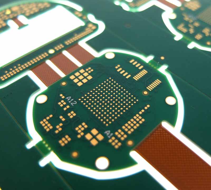
A rigid flex PCB is a printed circuit board that consists of rigid sections and flexible sections. The rigid sections provide structural support while the flexible sections allow the PCB to bend and flex. Rigid flex PCBs provide solutions for electronic devices that require dynamic movement, compact 3D packaging, and reduced system wiring. They are commonly used in aerospace, military, medical, automation, and consumer electronics applications.
Benefits of Rigid Flex PCBs
Here are some of the key benefits of using rigid flex PCBs:
- Dynamic flexing and bending – Allows movement in 3D space for applications like cameras, disk drives, robotic arms etc.
- Space savings – Fits and conforms inside irregular and tight spaces.
- Reduced system wiring – Flexible sections can replace wire harnesses and connectors.
- Increased reliability – Reduces mechanical stress and risk of failure.
- Design flexibility – Can integrate rigid and flexible sections in creative ways.
- Lightweight – Weighs less than using separate PCBs and connectors.
Rigid Flex Construction
A rigid flex PCB consists of the following components:
- Rigid layers – Usually FR-4 material that provides structure.
- Flexible layers – Usually polyimide that can bend dynamically.
- Bonding adhesive – Joins the rigid and flex layers.
- Coverlay/Mask – Protective coating over conductors.
The rigid and flexible layers are bonded together using adhesive films like acrylic or epoxy. The flexible sections allow the PCB to bend while the rigid sections prevent unwanted flexing. Specific rigid-flex constructions are chosen based on the required application.
Rigid Flex PCB Design Considerations
Designing a rigid flex PCB requires special considerations compared to designing a standard rigid PCB. Here are some of the main considerations:
Layer Stackup
The designer must determine the required number of conductive copper layers and dielectric material layers. Some key factors are:
- Number of signals to route
- Controlled impedance requirements
- Flexibility requirements
- Rigidity requirements
- High-speed signals requirements
A typical rigid-flex stackup has 2 to 12 conductive layers. At least one layer is used as a ground plane.
Flex Bend Areas
The flexing regions must be carefully planned considering:
- Bend radius – Avoid sharp folds that exceed minimum bend radius.
- Corners – Allow room for stress relief cutouts at bend corners.
- Dynamic flexing – Accommodate maximum dynamic flexing angle.
- Layers – Minimize the number of layers in the bend areas.
Transitions Between Rigid and Flex
The transitions between rigid and flexible sections require special considerations:
- Avoid sharp corners – Use rounded corners to reduce stress concentrations.
- Reinforce edges – Add additional material or increase thickness.
- Spread plating – Extend plated metallic layers into flex area.
- Backing support – Add stiffener materials to support flex.
Component Placement
Component placement on a rigid-flex PCB requires planning:
- Minimize components in flex area – Place mostly on rigid sections.
- Ensure clearance in bend areas – Provide space for dynamic flexing motion.
- Distribute weight evenly – Avoid lopsided weight distribution.
- Low profile components – Use flat components that do not protrude much.
PCB Thickness
The rigid sections are usually 0.031″ or 0.062″ thick. The flex sections are usually around 0.008″ to 0.012″ thick. The designer must choose appropriate thicknesses.
Rigid Flex PCB Manufacturing Process
Manufacturing rigid flex PCBs requires specialized processes compared to standard PCBs. Here is a general overview of the manufacturing process:
- Design – Create PCB layout in CAD software accounting for rigid-flex requirements.
- Prototyping – Make prototypes for design validation and testing.
- Layer fabrication – Fabricate individual conductive and dielectric layers.
- Lamination – Join layers using adhesive films through high heat and pressure.
- Drilling – Machine drill holes through rigid and flex areas.
- Metal coating – Plate exposed drill walls with copper to create plated through holes.
- Photoimaging – Apply photoresist coating and expose with circuit pattern artwork.
- Etching – Chemically etch away unwanted copper to leave intended circuit traces.
- Solder mask – Apply epoxy coating to protect traces from solder bridging and environmental damage.
- Silkscreen – Print reference designators, labels, and markings using ink.
- Testing – Test PCBs electrically and mechanically to validate proper function.
- Assembly – Populate boards with components using soldering or adhesive methods.
- Inspection – Verify assembly quality to meet specifications.
The specialized steps for rigid-flex boards involve the lamination, drilling, and handling processes that accommodate both rigid and flexible materials.
Rigid Flex PCB Materials
Here are the common materials used in rigid flex PCB fabrication:
| Material | Description |
|---|---|
| Polyimide | Flexible dielectric layers such as Kapton or UPILEX. Withstands repeated bending. |
| Acrylic adhesive | Bonds polyimide layers. Flexible when cured. |
| FR-4 | Rigid glass-reinforced epoxy layers. Provides structure. |
| Copper foils | Thin rolled copper sheets that form circuit traces after etching. |
| Coverlay | Flexible protective layer over traces. |
Rigid Flex PCB Design Software
Rigid flex PCBs require specialized CAD software to handle the combination of rigid and flexible sections in the design. Some popular options:
- Altium Designer – Provides specialized tools for trace routing, layer stack planning, flex modeling, and documentation.
- Cadence Allegro PCB Designer – Offers extensive rigid-flex features for layer stack design, flex modeling, and MCAD collaboration.
- Mentor Graphics Xpedition – Integrated tools for electrical, mechanical, and thermal modeling of complex rigid-flex boards.
- Zuken CR-8000 – Dedicated rigid-flex design suite with analysis and DFM features tailored for flex boards.
The CAD software should have capabilities to define rigid and flex regions, model dynamic bending, provide flex reliability analysis, and handle complex layer stackups.
Applications of Rigid Flex PCBs
Here are some common product applications that use rigid flex PCBs:
Aerospace and Defense
- Missiles – Interconnects that flex and bend within confined spaces
- Fighter jets – Boards that withstand vibration and repeated motion
- Avionics – Complex multilayer boards in tight spaces
Medical
- Hearing aids – Tiny interconnects that fit in the ear canal
- Surgical cameras – Flex boards that allow camera motion
- Patient monitors – Flexible wearable devices
Consumer Electronics
- Cell phones – Foldable and shape-changing designs
- Laptops – Interconnects between screen and keyboard
- Cameras – Boards that flex as lens focuses
- Wearables – Conformable boards for watches, glasses etc.
Automotive
- Sensors – Flex boards in engine compartments and chassis
- Infotainment – Displays that fold away when not used
- Lighting – Conformable PCBs integrated into curved headlights
Industrial
- Robotics – Arms and joints that require flexing interconnects
- Internet of Things – Flex sensor modules that adapt to environments
- Automation – Complex boards in tight spaces
FQA About Rigid Flex PCBs
Here are answers to some frequently asked questions about rigid flex PCBs:
Q: Why are rigid flex PCBs more expensive than standard PCBs?
A: The specialized materials, complex fabrication processes, lower production volumes, and additional testing required for rigid flex PCB manufacturing means they cost more than traditional rigid PCBs. But they provide unique benefits like flexibility, reliability, and space savings.
Q: How many times can a rigid flex PCB be flexed before failing?
A: The flex life depends on the materials and construction methods used. Typical rigid flex PCBs can withstand 500 to 10,000+ dynamic flexing cycles before traces start to crack or separate. Careful design and testing ensures sufficient flex life for the application.
Q: Can components be mounted directly on the flex section of a rigid flex PCB?
A: It is generally advised to mount components only on the rigid sections and avoid placing them in the flexible bend areas. Some exceptions are flat microchips that do not crack under bending. Flexible adhesives are used to attach such components.
Q: What are some best practices when designing rigid flex PCBs?
A: Some best practices include: avoid sharp corners or folds, distribute components evenly, use rounded transitions, allow clearance for dynamic motion, minimize layers in bend areas, analyze thermal stresses, and prototype/test designs thoroughly.
Q: How do you test a newly manufactured rigid flex PCB?
A: Electrical testing validates connectivity and function. Mechanical testing puts the board through repeat motion and vibration cycles to validate robustness. X-ray and AOI inspection ensures quality assembly. The testing depends on the end application requirements.