


Introduction
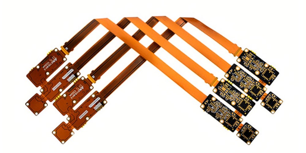
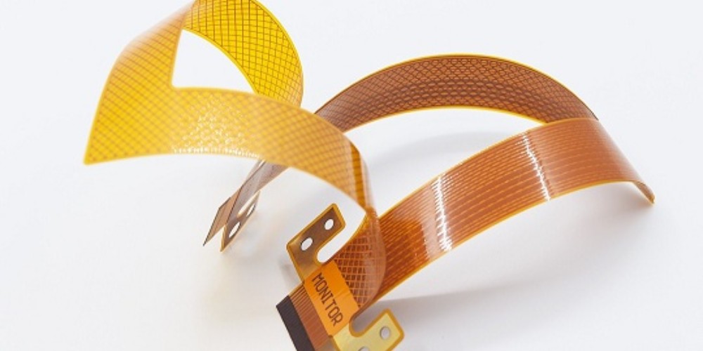
A flex PCB, also known as a flexible printed circuit board, is a type of PCB that can bend and flex. Flex PCBs allow circuitry to move freely and adapt to different environments. They are most commonly used in consumer electronics, medical devices, aerospace applications, and more. Flex PCBs provide several advantages over rigid PCBs including increased reliability, adaptability, and the ability to fit into tight or moving spaces.
Altium Designer is a leading PCB design software that provides all the features and tools needed for flex PCB design. This guide will cover the basics of designing flex PCBs with Altium, including:
- Flex PCB technology overview
- Benefits of flex PCBs
- Flex PCB design considerations
- Setting up flex stackups
- Routing flex PCBs
- Managing flex layers
- Checking flex assembly clearances
- Generating manufacturing outputs
Following this guide will provide the fundamental knowledge needed to start designing basic flex PCBs with Altium Designer.
Flex PCB Technology Overview
A flex PCB uses a flexible base material such as polyimide or polyester instead of the standard rigid FR-4 material. The flexible material allows the PCB to bend and flex repeatedly without breaking the copper traces.
The conductive layers are bonded to the flex base material through an adhesive film. A coverlay (solder mask) is added on top of the outer copper layers for protection. Flex PCBs typically have between 1 to 12 conductive layers.
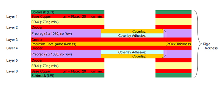
Cross section of a typical flex PCB layer stackup
Flex PCBs can have sections of rigid FR-4 called “rigid islands” that provide mounting stability for connectors or components. Vias and holes on flex PCBs require special attention to avoid cracking during movement.
Overall, the flexible construction allows flex PCBs to take on unique form factors and move dynamically in ways not possible with rigid boards.
Benefits of Flex PCBs
There are several notable benefits that make flex PCBs an attractive option:
- Adaptability – The flexible nature allows flex PCBs to fit into tight spaces, bend around components, and adapt to complex geometries. This allows for packaging innovations not possible with rigid PCBs.
- Reliability – Flex PCBs are extremely durable against vibration and flexion stresses. The flexing motion actually works to relieve strain on solder joints, increasing reliability.
- Lightweight – Flex PCBs use thinner base materials than rigid PCBs, making them extremely lightweight. This allows them to move freely and be ideal for portable devices.
- High Speeds – Carefully designed flex PCBs can support high speed signals comparable to rigid boards due to the shorter trace lengths.
- Design Freedom – Flex PCB technology enables endless design innovations and shapes not feasible with rigid technology. Curved and 3D flex PCBs open new possibilities.
Overall, flex PCB technology brings reliability, adaptability, and design freedom to electronic circuits in a lightweight, dynamic package. These benefits make flex PCBs an essential option for many modern devices and applications.
Flex PCB Design Considerations
Designing a successful flex PCB requires accounting for some unique considerations:
- Flexible Bends – Avoid sharp 90 degree bends and instead design smooth curves and bends in the 3D path of the flex PCB. Sharp bends create stress points.
- Layer Stacking – Stagger the placement of outer layer copper fills slightly to avoid having stiff sections that impair bending. Stack critical signals closer to the center.
- Component Placement – Place components in rigid sections of the PCB or at the neutral centerline of flexing areas. Avoid placing components in extreme flexing regions.
- Trace Routing – Route traces perpendicular to the bend axis and avoid traces running parallel to the bend. Use zig-zag or meandered traces to improve bend tolerance.
- Vias – Only use stacked and filled vias, avoid through-hole vias. Ensure vias have sufficient annular rings for flexibility.
- Stiffeners – Add stiffening materials or rigid sections judiciously. Too much stiffening impairs flexing action.
Taking these guidelines into account will lead to a flex PCB that bends as intended without damaging traces or components.
Setting Up Flex Stackups
A key first step in Altium is configuring the proper layer stackup. This defines the layer materials, sequence, and key attributes.
To create a new flex stackup:
- Open the Layer Stack Manager from the Layer Stack folder in the Projects panel.
- Choose File > New > Layer Stack to create a blank stackup file.
- Enter a name for the new layer stack.
- Define layer types, materials, thicknesses, and sequence order.
- Add flex core layers like polyimide.
- Include flexible coverlay layers.
- Optionally create stiffener layers.
- Assign copper layers to conductors (Signal, Plane, Dielectric).
- Set attributes like layer color, font size, etc.
- Save the layer stack.
Once defined, the flex layer stackup can be added to a PCB document by selecting from the Layer Stack Manager panel during creation.
With the proper flex layer stack loaded, you can begin laying out flex PCB designs.
Routing Flex PCBs in Altium
Routing traces and signals on a flex PCB follows the same process as rigid PCB routing in Altium. However, there are some settings and strategies to keep in mind for flex PCB designs:
- Teardrop Pads – Enable teardrop pads on all pad shapes to improve flexing strain relief.
- Trace Width – Use wider trace widths than the minimum requirement to improve flex lifespan.
- Rounded Corners – Use rounded corners on all trace angles and pad connections for flexibility.
- No Acute Angles – Avoid traces meeting at acute angles, instead use obtuse angles for connections.
- Perpendicular Routing – Route traces perpendicular to the bend axis whenever possible.
- Staggered Planes – Slightly offset signal and plane layers from each other for best bendability.
- 45 Degree Bends – Route traces in 45 degree bend segments instead of 90 degree angles.
- No Rigid-Flex Overlap – Don’t route traces from rigid to flex sections, instead route to a pad then connect.
Following these guidelines while routing will result in reliable, durable flex PCB traces.
Managing Flex Layers in Altium
Since flex PCBs contain both flexible layers and rigid sections, managing the layers and their constraints is important in Altium.
The core methods for managing flex layers include:
- Bending Lines – Draw bending lines to define the fold axes and location of bends.
- Rigid-Flex – Use the Rigid-Flex mode to define rigid sections and set isolation margins between rigid and flex areas.
- Mechanical Layers – Add mechanical layers to define rigid sections, stiffeners, bonded layers, and coverlay cutouts.
- Length Tuning – Adjust layer lengths in the Layer Stack Manager to ensure correct rigid/flex lengths.
- Rule Checks – Run the Flexural Stress rule check to verify traces can tolerate bend strains.
Properly configuring the layers and rigid/flex regions ensures the design bends and performs as expected.
Checking Flex Clearances
In addition to electrical clearance rules, flex PCBs also require special checks for assembly clearances.
Some important clearance rules to validate include:
- Component Clearance – Verify clearance between components in flexed and unflexed positions.
- Fold Clearance – Check for adequate clearance around bends and folds in the flex PCB profile.
- Panel Clearance – Ensure sufficient clearance between boards on the manufacturing panel.
- Hole Alignment – Confirm holes across rigid-flex boundaries still align when flexed.
- Case Fit – Model the 3D clearance between flex PCB and surrounding case or enclosure.
Running these analysis rules will avoid collisions and impediments when the flex PCB is integrated and operational.
Generating Manufacturing Outputs
Once the flex PCB design is complete, the last step is generating the manufacturing outputs.
Some key outputs include:
- Gerber Files – Standard 2D fabrication data for PCB production.
- Assembly Drawings – Drawings showing components, callouts, and critical dimensions.
- 3D PDF – 3D PDF with a bending model to visualize the flexed PCB profile.
- Drill Files – NC drill files for drilled hole locations.
- BOM – Bill of materials listing all components to procure.
- Fabrication Drawings – Details on board shape, cutouts, special features, etc.
Carefully going through outputs ensures the board house has all data required to produce your flex PCB design correctly.
Conclusion
Using Altium Designer provides a robust, capable toolset for designing functional flex PCBs. Following the guidelines and strategies outlined in this guide will enable you to leverage the benefits of flex PCB technology and integrate them into your devices. With the right know-how, flex PCBs can be designed efficiently. The unique advantages unlocked by flex PCBs make them a key enabling technology for next-generation electronics.
FQA
What are some typical applications for flex PCBs?
Some common applications that benefit from using flex PCBs include:
- Wearable devices – By bending and flexing with the body.
- Mobile phones – Allowing the circuitry to wrap around and fit in tight spaces.
- Medical instruments – Snaking into the contours of the human body.
- Automotive – Withstanding vibration while providing dynamic movement.
- Robotics – Allowing movement of joints while protecting circuits.
- Aerospace – Incorporating dynamic shapes while enduring G forces.
What are some best practices for routing high speed signals on flex PCBs?
Some routing tips for high speed signals on flex PCBs:
- Keep signals as short and straight as possible.
- Maintain proper impedance matching and controlled impedance routes.
- Avoid 90 degree turns, use two 45 degree turns instead.
- Route critical signals close to center or neutral bend axis when possible.
- Use wider trace widths than the minimum required for better signal integrity.
- Add ground planes adjacent to signal layers for shielding.
- Increase clearances between high speed traces to minimize crosstalk.
How are components typically mounted on flex PCBs?
The most common flex PCB component mounting methods include:
- Through-hole – Leaded components mounted into plated through holes. Requires rigid section of PCB.
- SMT – Surface mount components applied on flex PCB surface. May require adhesive or clamping.
- Sockets – Place female sockets on rigid islands, flex PCB plugs into socket.
- Cutouts – Strategic openings in flex PCB allow placing components on separate rigid PCB underneath.
- Encapsulation – Sensitive components can be completely encapsulated and attached to flex PCB.
What manufacturing and assembly challenges are unique to flex PCBs?
Some key manufacturing and assembly challenges with flex PCBs include:
- Achieving consistent bends and shapes without cracking.
- Tolerancing and aligning layers/features through bending sections.
- Dealing with dimensional instability and shrinkage of flex materials.
- Applying protective coverlay accurately over all copper edges.
- Assembly and soldering components effectively onto flexible substrate.
- Aligning and fastening components in both flexed and unflexed orientations.
- Providing adequate strain relief on traces, pads, and leads.
- Preventing handling damage to flexible materials during production.
What are some considerations for designing rigid-flex transition zones?
Here are some best practices for rigid-flex transition zones:
- Use a stepped tapered section for the transition instead of an immediate junction.
- Alternate layers of stiffeners on outer layers with flexible core material.
- Ensure at least 75% of layer materials are common between rigid and flex areas.
- Avoid placing plated through holes right at the transition interface.
- Use slits or curved voids at the transition to relieve stresses.
- Route no traces spanning the rigid-flex boundary. Use pads and short jumpers instead.
- Minimize component density on layers crossing the transition.
- Add solder mask web tenting for reliability.
Following these tips will create robust, reliable transitions between rigid and flex sections on the PCB.