

Introduction to Flex Circuits
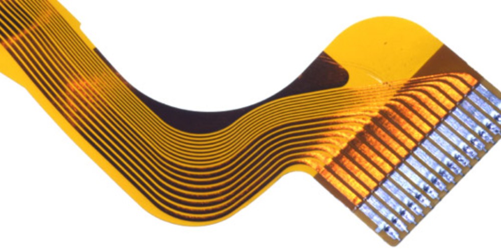
A flex circuit, also known as a flexible printed circuit board (PCB), is a type of circuitry made with flexible materials such as polyimide films. Unlike traditional rigid PCBs, flex circuits can bend, twist, and flex dynamically without damage during use. This makes them ideal for manufacturing compact electronics that require movable or pliable circuits, like medical devices, wearables, IoT products, and consumer electronics.
Flex circuits provide a number of benefits over rigid boards:
- Flexible form factors – can be bent, folded or twisted to fit product shapes
- Lightweight and thin – reduces product weight and size
- Durable under dynamic motion – flexing doesn’t crack solder joints
- Efficient wiring between components – replaces loose wires and connectors
- Reliable connections – circuits remain stable during motion
- Scalable manufacturing – can be mass produced efficiently
However, flex circuit design also comes with challenges not found in rigid PCBs. Engineers must account for factors such as dynamic flexing, thermal expansion, impedance control, and material stability over product lifetimes.
This guide provides a comprehensive overview of flex circuit design, materials, manufacturing, and assembly processes. It covers key considerations and best practices for designing robust, reliable flex circuits.
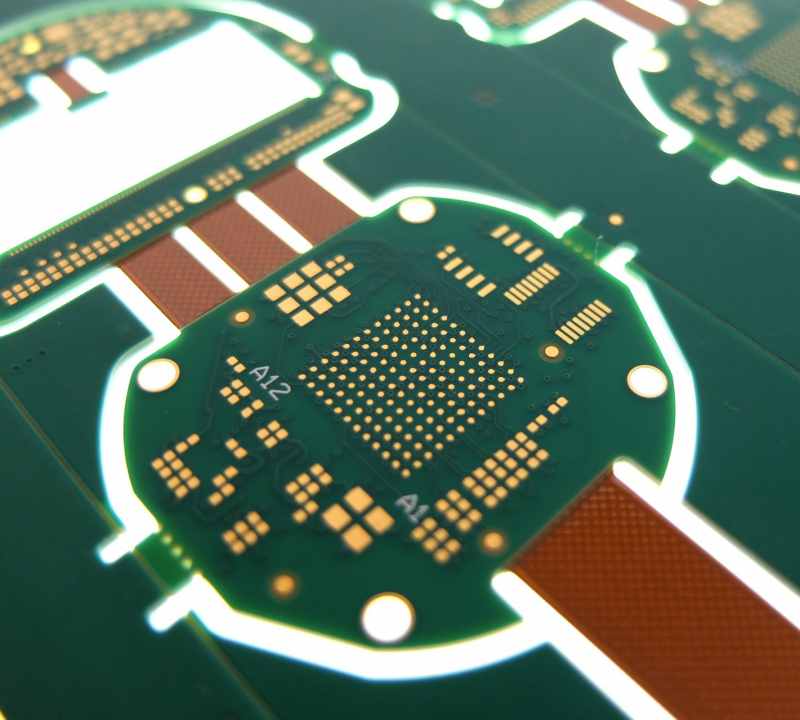
Flex Circuit Materials and Construction
Flex circuits consist of conductive traces and pads etched from copper laminated onto a polymer substrate film. The most common substrate material is polyimide (e.g. Kapton) which provides excellent thermal stability and chemical resistance. Other polymer films used include PET, PEN, and polyester.
The basic construction of a flex circuit includes:
- Base Substrate – Thin polymer film that provides the foundation. Common thickness range is 12.5-125um.
- Conductive Layer – Copper foil, typically 18-35um thick, laminated onto substrate.
- Photoresist – Light-sensitive polymer coating that is imaged to form circuit pattern.
- Coverlay – Polyimide overlay that insulates and protects conductive traces.
- Stiffeners – Added rigid sections for mounting components or connectors.
- Cover Coat – Optional insulative final coating for environment protection.
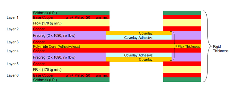
Cross-section of a typical flex circuit construction
Flex stackups with multiple conductive layers are also possible for more complex circuits. Common manufacturing techniques used include:
- Photolithography – imaging circuit traces with UV light
- Etching – chemically dissolving unwanted copper
- Lamination – bonding layers with heat and adhesive films
- Drilling – creating plated through-holes for vias
Flex Circuit Design Rules and Guidelines
Designing a reliable flex circuit requires adhering to specific guidelines regarding trace geometries, spacing, materials, and layout:
Trace Width/Space
- Minimum trace width: 0.10mm (4mil)
- Minimum trace spacing: 0.10mm (4mil)
Narrower traces are prone to broken circuits either during flexing or PCB fabrication process.
Bend Radius
- Minimum bend radius: Thickness x 10
- Dynamic flexing: Radius x 100
Sharp folds generate high strains that can fracture copper and degrade polymer.
Copper Thickness
- 1 oz (35um) foil is typically used
- 2 oz (70um) may be used for high-current
Thick copper is prone to cracking along trace edges when folded.
Stiffeners
- Use rigid stiffeners around connectors and components
- Reduce stiffener thickness if located in bend area
Stiff sections restrict flexibility – can delaminate or fracture if overly stiff.
Annular Rings
- Pads/vias should have ≥ 0.10mm annular ring
- Accounts for misregistration during drilling
Insufficient annular ring risks cracked/open pads or shorts.
Adhesives
- Use supported or non-flowing adhesive films
- Avoid liquid adhesives
Flowing adhesives increase thickness, restrict bending, and risk short circuits.
By following these design guidelines, flex circuits can achieve tight spacing for routing while remaining flexible and robust under repeated dynamic bending motions.
Considerations for Dynamic Flex Circuits
For applications requiring continuous flexing motions, additional design considerations are necessary to ensure flex circuit reliability:
Dynamic Bend Radius
- Increase minimum radius to limit strain
- Radius ≥ 100 x material thickness
Prevents metal fatigue and trace fracturing over product lifetime
Trace Orientation
- Run traces perpendicular to bend axis
- Avoid traces spanning across bend areas
Lessens risk of broken circuits due to repeated cyclic stresses
Termination Pads
- Use tear-drop shaped pads at trace ends
- Avoid thin rectangular pads
Reduces stress concentrations to prevent pad lift-off and delamination
Flex Service Loop
- Route extra trace lengths in bend areas
- Allows traces to flex without damage
Polymer Creep
- Select substrate materials with low creep
- Reinforce with non-woven glass fiber
Minimizes insulation elongation and potential short circuits.
Conformal Coatings
- Coat circuitry to prevent cracks
- Paralyne, urethane, silicone options
Protects against environmental exposure and dendrite growth
With careful material selection and design strategies focused on flex durability, dynamic flex circuits can achieve millions of cycles and long working lifetimes.
Flex Circuit Assembly and Connectors
Properly integrating components, connectors, and mounting interfaces is critical for creating usable flex circuit assemblies:
Component Mounting
- Adhere components withflexible adhesives
- Avoid rigid epoxies
Flex adhesives accommodate movement and thermal expansion mismatches.
Connectors
- Use flex-tail connectors
- Provide sufficient strain relief
Rigid connectors restrict and concentrate flex stresses.
Bond Pads/Solder Mask
- Define bond pads for adhesives/solder
- Cover other areas with solder mask
Provides electrical isolation and environmental protection.
Corner Terminations
- Use rounded, tear-drop pads
- Avoid 90° angles
Reduces stress points vulnerable to cracking and lift-off.
Reinforcements
- Add non-woven fabric layers
- Shield against cuts and punctures
Maintains circuit integrity under extreme flexing or abrasion.
Shielding
- Use metallic layer for EMI shielding
- Careful design for flexibility
Blocks unwanted electromagnetic interference.
Proper assembly methods enable the advantages of flex circuits to be utilized in the finished circuit board. Factors like stress relief, flexible attachments, and abrasion resistance must be considered.
Applications of Flexible Circuits
The unique properties of flex circuits make them well-suited for the following applications:
Wearable Electronics
- Ability to conform to body and clothing
- Lightweight and comfortable
- Washable and durable
Used in smartwatches, fitness trackers, health sensors
Medical Devices
- Dynamic flex life for implants
- Chemical resistance
- Sterilizable
Found in patient monitors, pumps, surgical tools
Consumer Electronics
- Compact, movable joints
- Space and weight savings
- Simplified assembly
Used in laptops, phones, cameras, and appliances
Automotive
- Vibration resistance
- Withstands temperature swings
- Low-profile routing
Used in sensors, cameras, lighting, control modules
Aerospace/Military
- Extreme environment tolerance
- Reliability under vibration
- EMI/RFI shielding
Used in guidance systems, controls, engine monitoring
Robotics
- Flexible hinges and joints
- Simplified cable routing
- Rugged for motion and abrasion
Located in arms, joints, end effectors
The combination of flexibility, reliability, and design versatility makes flex circuits an enabling technology across many industries pushing the boundaries of electronic devices and systems.
Key Takeaways on Flexible PCB Design
Some of the key points to remember when designing flex circuits include:
- Adhere to minimum bend radius and trace dimensions
- Orient traces properly to bend axis
- Use generous fillets on pads and traces
- Allow for service loop lengths in dynamic areas
- Select robust, flex-tested materials
- Plan design for flex assembly methods
- Incorporate features for environmental protection
- Partner with experienced flex circuit manufacturers
By following best practices for flexible PCB layout and manufacture, engineers can take full advantage of the benefits of flex circuits while mitigating inherent design challenges. With upfront planning and careful validation, flex circuits enable custom-molded electronics that can survive millions of cycles under demanding mechanical requirements.
Flex Circuit Design FQA
1. What are the main benefits of using flex circuits versus rigid boards?
Some key advantages of flex circuits over rigid boards include:
- Dynamic flexibility without damage
- Thinner, lighter, and more compact
- Tight component layouts and routing
- Simplified cabling and connections
- Vibration dampening and improved reliability
- Conforms to complex product shapes
- Easier prototyping and design modifications
2. What characteristics of materials should be evaluated for robust flex circuit design?
Important flex circuit material properties to evaluate include:
- Flexibility – bending radius and modulus
- Thermal stability – operating temp range
- Chemical resistance – compatibility with applications
- Dielectric strength – insulation properties
- Creep resistance – avoids trace shorting
- Adhesion – between polymer layers
- Flammability – for safety
Polyimide films tend to have a good balance of these properties.
3. How are components typically attached to flex circuits?
Common component attachment methods include:
- Conductive adhesives – flexible, withstands shock/vibe
- SMT soldering – can require stress relief
- Mechanical fasteners – screws, clips
- Plated through-holes – with annular ring
Avoid rigid attachments or epoxies that could crack.
4. What are some ways to improve reliability in dynamic flexing areas?
Strategies for improving flex circuit reliability include:
- Wider trace widths and spacing
- Flexible adhesives and solder mask
- Additional polymer layers for insulation
- Fiber reinforcement for abrasion resistance
- Rounded, tear-drop component pads
- Service loops to reduce trace stresses
5. How are Shields incorporated into flex circuits?
Common methods for EMI shielding include:
- Laminated metal foil layer – flexible if thin
- Conductive adhesive or gasket
- Metallic enclosure or stiffener
- Conductive coatings like silver ink
- Plated through-hole vias for shielding
Careful design is needed to maintain flexibility.