

Introduction to Circuit-Drawing
Circuit-drawing is an essential skill for anyone interested in electronics, whether you’re a hobbyist or a professional engineer. Drawing a circuit board allows you to visualize the connections between components, plan the layout of your project, and create a blueprint for manufacturing. In this article, we’ll guide you through the process of drawing a simple circuit board, from understanding the basic components to using software tools for more complex designs.
What is a Circuit Board?
A circuit board, also known as a printed circuit board (PCB), is a flat board made of insulating material, such as fiberglass or plastic, with conductive pathways etched onto its surface. These pathways, called traces, connect various electronic components, such as resistors, capacitors, and integrated circuits (ICs), to form a functional electronic device.
Why Draw a Circuit Board?
Drawing a circuit board is an important step in the design process of an electronic device. It allows you to:
- Visualize the connections between components
- Plan the layout of your project
- Create a blueprint for manufacturing
- Identify potential issues before building the actual device
- Communicate your design to others
Understanding the Basic Components
Before you start drawing a circuit board, it’s essential to understand the basic components that make up a circuit. These components include:
Resistors
Resistors are passive components that limit the flow of current in a circuit. They are represented by a zigzag line in schematic diagrams and are labeled with their resistance value in ohms (Ω).
Capacitors
Capacitors store electrical energy in an electric field. They are represented by two parallel lines in schematic diagrams and are labeled with their capacitance value in farads (F).
Inductors
Inductors store electrical energy in a magnetic field. They are represented by a coil or a series of loops in schematic diagrams and are labeled with their inductance value in henries (H).
Diodes
Diodes are semiconductor devices that allow current to flow in only one direction. They are represented by a triangle pointing towards a line in schematic diagrams and are labeled with their part number or type.
Transistors
Transistors are semiconductor devices that can amplify or switch electronic signals. They are represented by a symbol with three terminals (base, collector, and emitter) in schematic diagrams and are labeled with their part number or type.
Integrated Circuits (ICs)
Integrated circuits are miniaturized electronic circuits that contain multiple components, such as transistors, resistors, and capacitors, on a single chip. They are represented by rectangular boxes with multiple pins in schematic diagrams and are labeled with their part number or function.

Drawing a Schematic Diagram
Before drawing the actual circuit board, it’s crucial to create a schematic diagram that represents the electrical connections between the components. A schematic diagram uses standardized symbols to represent the components and shows how they are connected, without regard to the physical layout of the circuit board.
Steps to Draw a Schematic Diagram
- Identify the components needed for your circuit
- Draw the power supply and ground symbols
- Place the components on the diagram, using the appropriate symbols
- Connect the components with lines representing the electrical connections
- Label the components with their values or part numbers
- Add any necessary notes or annotations
Tips for Drawing a Schematic Diagram
- Keep the diagram clean and organized
- Use a consistent labeling system
- Group related components together
- Use net names to label important connections
- Include a title, date, and revision number

Drawing the Circuit Board Layout
Once you have a schematic diagram, you can start drawing the actual circuit board layout. The layout shows the physical arrangement of the components and the traces that connect them.
Steps to Draw a Circuit Board Layout
- Determine the size and shape of the circuit board
- Place the components on the board, using the schematic diagram as a reference
- Route the traces between the components, following the electrical connections in the schematic
- Add any necessary vias (holes that connect traces on different layers)
- Add Mounting holes and any other mechanical features
- Add a silkscreen layer with component labels and other markings
Tips for Drawing a Circuit Board Layout
- Keep the layout compact and efficient
- Minimize the length of traces to reduce signal interference
- Use a ground plane to reduce noise and improve signal integrity
- Follow the manufacturer’s recommended footprints for components
- Use a grid to align components and traces
- Follow any design rules specified by the PCB manufacturer

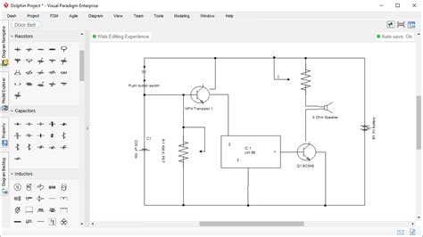
Using Software Tools for Circuit-Drawing
While it’s possible to draw simple circuit boards by hand, most modern designs are created using specialized software tools. These tools allow you to create schematic diagrams, design PCB Layouts, and generate files for manufacturing.
Popular Circuit-Drawing Software
| Software | Description | Operating System |
|---|---|---|
| KiCad | Free and open-source EDA software suite | Windows, macOS, Linux |
| Eagle | Popular EDA software with a free version for small boards | Windows, macOS, Linux |
| Altium Designer | Professional-grade EDA software with advanced features | Windows |
| OrCAD | Comprehensive EDA software suite for complex designs | Windows |
| Fritzing | Beginner-friendly EDA software with a focus on Arduino projects | Windows, macOS, Linux |
Advantages of Using Software Tools
- Easier to create and modify complex designs
- Built-in libraries of component symbols and footprints
- Automated design rule checking (DRC) to catch errors
- Ability to generate files for manufacturing (Gerber, drill, BOM, etc.)
- Collaboration features for working with a team
Finalizing Your Circuit Board Design
Before sending your circuit board design for manufacturing, it’s important to review and finalize your design.
Design Review Checklist
- Double-check the schematic diagram for accuracy
- Verify that the PCB layout matches the schematic
- Ensure that all components are properly placed and oriented
- Check for any design rule violations (DRC errors)
- Review the manufacturability of the design with the PCB fabricator
- Create a bill of materials (BOM) for ordering components
Generating Manufacturing Files
Once your design is finalized, you’ll need to generate the necessary files for manufacturing. These files typically include:
- Gerber files: The industry-standard format for PCB Fabrication data
- Drill files: Specifies the location and size of holes in the PCB
- Bill of Materials (BOM): A list of all components used in the design
- Assembly drawings: Shows the placement and orientation of components on the PCB
Most circuit-drawing software tools can generate these files automatically, but it’s essential to review them for accuracy before submitting them to the manufacturer.
Frequently Asked Questions (FAQ)
- What is the difference between a schematic diagram and a PCB layout?
- A schematic diagram represents the electrical connections between components, while a PCB layout shows the physical arrangement of components and traces on the circuit board.
- Can I draw a circuit board by hand?
- Yes, it’s possible to draw simple circuit boards by hand, but most modern designs are created using specialized software tools for accuracy and efficiency.
- What are the advantages of using software tools for circuit-drawing?
- Software tools make it easier to create and modify complex designs, provide built-in libraries of component symbols and footprints, offer automated design rule checking, and generate files for manufacturing.
- What files do I need to provide to the PCB manufacturer?
- Typically, you’ll need to provide Gerber files, drill files, a bill of materials (BOM), and assembly drawings to the PCB manufacturer.
- How do I ensure my circuit board design is manufacturable?
- Review your design with the PCB fabricator, ensure that all components are properly placed and oriented, check for design rule violations, and generate accurate manufacturing files.
Conclusion
Drawing a simple circuit board is a crucial skill for anyone interested in electronics. By understanding the basic components, creating a schematic diagram, and drawing the PCB layout, you can bring your electronic projects to life. Using software tools can streamline the design process and help you create more complex and efficient designs. With practice and attention to detail, you’ll be able to design and manufacture your own custom circuit boards.