

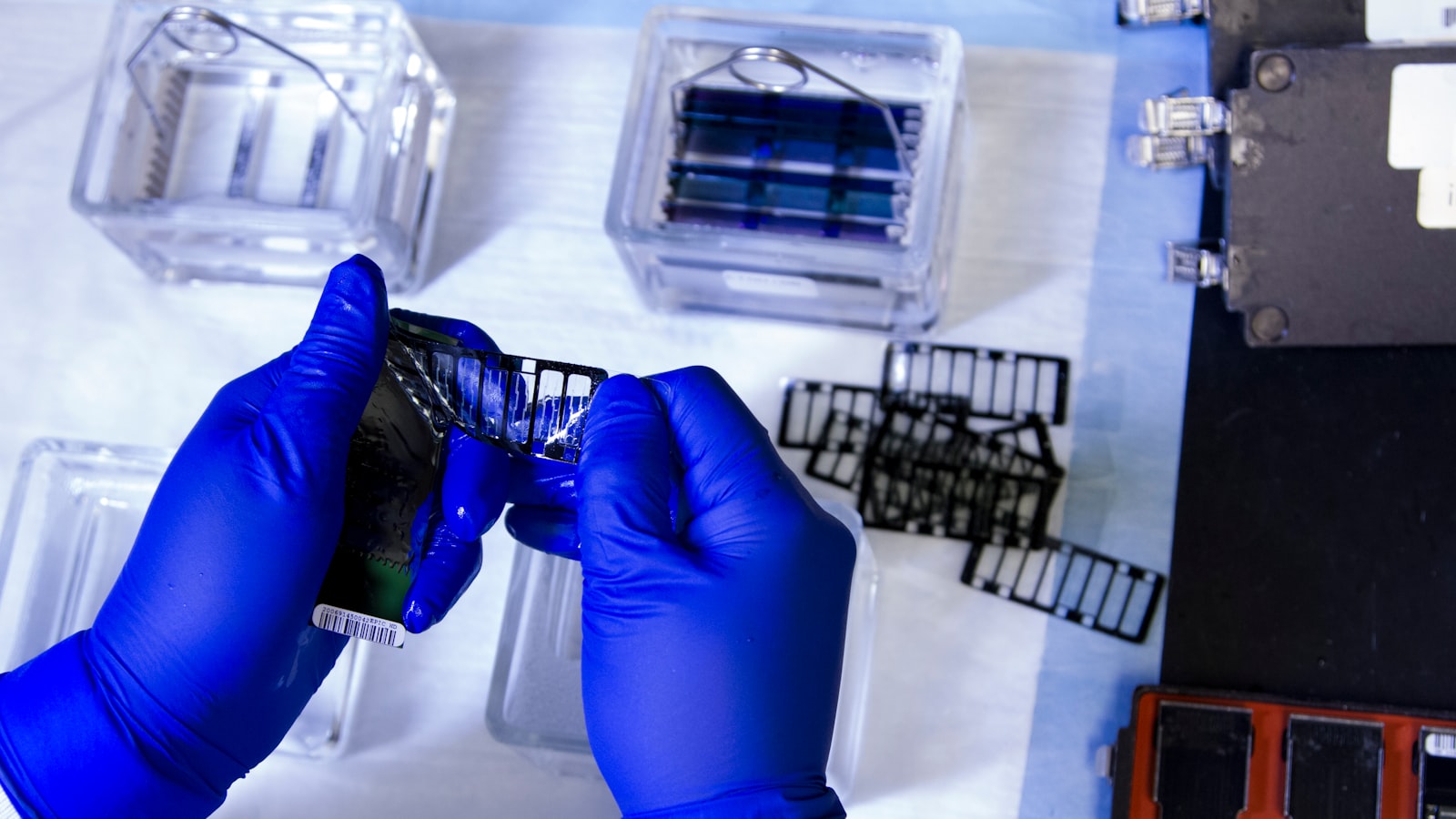
What is PCB Testing?
PCB testing is the process of verifying the functionality, quality, and reliability of a printed circuit board. It involves various techniques to ensure that the PCB is free from defects, such as short circuits, open circuits, incorrect component placement, and manufacturing flaws. PCB testing is essential to maintain the quality of the final product and prevent potential failures in the field.
Why is PCB Testing Important?
PCB testing is crucial for several reasons:
-
Quality Assurance: Testing helps identify defects and manufacturing flaws early in the production process, allowing for timely corrections and reducing the risk of faulty products reaching the market.
-
Reliability: Thorough testing ensures that the PCBs will function as intended and maintain their performance over time, enhancing the reliability of the final product.
-
Cost Savings: Detecting and fixing issues during the testing phase is more cost-effective than dealing with product returns, repairs, or replacements after the product has been released.
-
Compliance: PCB testing helps ensure that the boards meet industry standards and regulatory requirements, such as safety, electromagnetic compatibility (EMC), and environmental regulations.

7 PCB Testing Methods
1. In-Circuit Testing (ICT)
In-Circuit Testing is a powerful and widely used PCB testing method that verifies the functionality of individual components and their interconnections on the board. ICT is performed using a specialized test fixture that makes direct contact with the PCB through a bed of nails or probes.
How In-Circuit Testing Works
- The PCB is placed on the test fixture, and the probes make contact with the test points on the board.
- The ICT system applies electrical signals to the components and measures their responses.
- The measured values are compared against the expected values defined in the test program.
- Any discrepancies indicate a fault, such as a short circuit, open circuit, or incorrect component value.
Advantages of In-Circuit Testing
- Provides comprehensive coverage of component-level faults
- Can detect manufacturing defects and component failures
- Offers high test throughput and fast test times
- Enables easy fault diagnosis and repair
- Suitable for high-volume production
Limitations of In-Circuit Testing
- Requires custom test fixtures, which can be expensive
- Limited access to dense or miniaturized PCBs
- May not detect certain functional or performance issues
2. Functional Testing
Functional testing verifies that the PCB performs its intended functions as per the design specifications. It involves applying input signals to the board and measuring the output response to ensure proper operation.
Functional Testing Methods
- Edge Connector Testing: Involves connecting the PCB to a test system through its edge connectors and applying test signals.
- Boundary Scan Testing: Uses built-in test circuitry (JTAG) to test the interconnections and functionality of digital components.
- Flying Probe Testing: Employs movable probes to contact test points on the PCB and perform functional tests.
3. Automated Optical Inspection (AOI)
AOI uses high-resolution cameras and image processing algorithms to inspect the PCB for visual defects, such as incorrect component placement, solder bridging, or missing components.
4. X-Ray Inspection
X-ray inspection is used to detect hidden defects, such as voids in solder joints, insufficient solder coverage, or misaligned components, which are not visible through visual inspection.
5. Burn-In Testing
Burn-in testing involves subjecting the PCB to elevated temperatures and electrical stress for an extended period to identify early failures and ensure the board’s reliability under adverse conditions.
6. Boundary Scan Testing
Boundary scan testing, also known as JTAG testing, utilizes built-in test circuitry to test the interconnections and functionality of digital components on the PCB. It enables testing of hard-to-reach components and provides diagnostic capabilities.
7. Flying Probe Testing
Flying probe testing uses movable probes to contact test points on the PCB and perform electrical tests. It offers flexibility in testing complex boards and is suitable for low-volume production or prototype testing.
Comparison of PCB Testing Methods
| Testing Method | Detects | Test Coverage | Test Speed | Cost |
|---|---|---|---|---|
| In-Circuit Testing (ICT) | Component-level faults, manufacturing defects | High | Fast | High |
| Functional Testing | Functional issues, performance problems | Medium to High | Medium | Medium |
| Automated Optical Inspection (AOI) | Visual defects, component placement issues | High | Fast | Medium |
| X-Ray Inspection | Hidden defects, solder joint issues | High | Medium | High |
| Burn-In Testing | Early failures, reliability issues | Low to Medium | Slow | Medium |
| Boundary Scan Testing | Interconnection faults, digital component functionality | Medium to High | Fast | Medium |
| Flying Probe Testing | Electrical faults, prototype testing | Medium | Slow | Medium |
Frequently Asked Questions (FAQ)
1. What is the difference between In-Circuit Testing and Functional Testing?
In-Circuit Testing focuses on verifying the functionality of individual components and their interconnections, while Functional Testing verifies the overall functionality of the PCB as per the design specifications.
2. Can In-Circuit Testing detect all types of PCB defects?
In-Circuit Testing is effective in detecting component-level faults and manufacturing defects. However, it may not detect certain functional or performance issues that require the entire board to be tested as a system.
3. Is Automated Optical Inspection sufficient for ensuring PCB quality?
While AOI is highly effective in detecting visual defects and component placement issues, it cannot detect hidden defects or electrical faults. Therefore, AOI should be used in conjunction with other testing methods for comprehensive quality assurance.
4. When is X-Ray Inspection necessary for PCB testing?
X-Ray Inspection is necessary when there are hidden defects or issues with solder joints that cannot be detected through visual inspection. It is particularly useful for inspecting high-density boards or components with hidden connections.
5. How does Boundary Scan Testing differ from other PCB testing methods?
Boundary Scan Testing utilizes built-in test circuitry (JTAG) to test the interconnections and functionality of digital components. It offers the advantage of testing hard-to-reach components and provides diagnostic capabilities without the need for physical access.
Conclusion
PCB testing is a vital aspect of the electronics manufacturing process, ensuring the quality, reliability, and functionality of the final product. Among the various testing methods, In-Circuit Testing stands out as a comprehensive and widely used technique for detecting component-level faults and manufacturing defects.
However, to achieve optimal results, it is essential to employ a combination of testing methods based on the specific requirements of the PCB and the product. By implementing a robust testing strategy that includes In-Circuit Testing, Functional Testing, AOI, X-Ray Inspection, and other relevant methods, manufacturers can ensure the highest quality standards and deliver reliable products to their customers.
As PCB technology continues to evolve, with increasing complexity and miniaturization, the importance of effective testing methods will only grow. Investing in advanced testing equipment, skilled personnel, and continuous process improvement will be key to staying competitive in the ever-changing landscape of electronics manufacturing.