

What is the difference between track and trace in PCB?
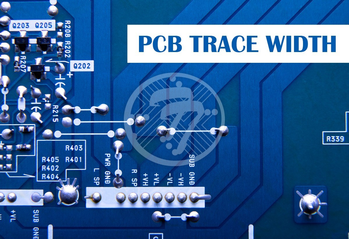
Introduction to PCBs
A printed circuit board (PCB) is a board made of fiberglass, composite epoxy, or other insulating material, used to mechanically support and electrically connect electronic components using conductive pathways or traces etched from copper sheets laminated onto a non-conductive substrate. PCBs provide the mechanical structure to mount and interconnect electronic components.
PCB Tracks and Traces
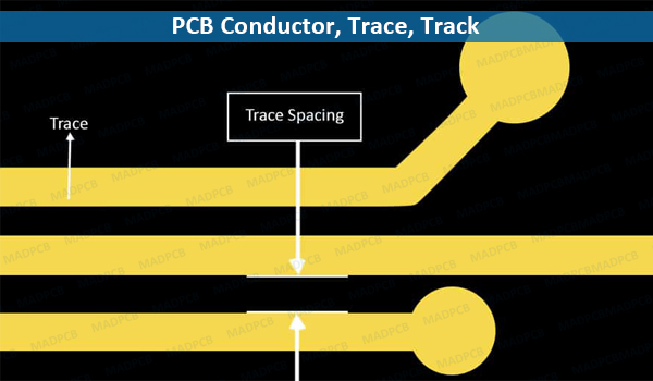
The conductive pathways on a PCB that carry signals between components are generally referred to as either “tracks” or “traces”. These terms are often used interchangeably, but there are some subtle differences:
Tracks usually refer to the wider pathways on a PCB, often those that provide power or ground connections. Tracks are sometimes defined as conductive pathways greater than 20 mils (0.02 inches) in width.
Traces usually refer to the thinner conductive pathways that carry signals between components. Traces are sometimes defined as conductive pathways less than 20 mils in width.
So in summary:
- Tracks – Wider pathways, usually for power or ground
- Traces – Thinner pathways for signals
But in general conversation, the words track and trace are often used interchangeably when referring to the conductive copper pathways on a PCB.
PCB Trace Design Considerations
There are several important considerations that go into designing PCB traces:
Trace Width
The width of a trace determines the amount of current it can safely carry without overheating. Wider traces can carry more current. Trace width also affects resistance, with wider traces having lower resistance. Some key calculations help determine appropriate trace widths.
Current Carrying Capacity
Every PCB trace has a maximum current carrying capacity which depends on:
- Trace width – Wider traces can carry more current
- Trace thickness – Thicker copper has higher current capacity
- Ambient air temperature – Ability to dissipate heat
- PCB copper weight – Heavier copper has higher thermal conductivity
Exceeding the current carrying capacity can lead to overheating and possibly failure. Specifications provide maximum current ratings for different PCB parameters.
Trace Length
The total trace length impacts resistance and affects the transmission of high speed signals:
- Longer traces increase resistance which causes unwanted voltage drops
- Long traces increase capacitance and impedance discontinuities which distort high speed signals
So in high speed designs, trace lengths should be kept as short as possible.
Trace Routing
Trace routing refers to the paths taken to route traces between pins and components on the PCB. Good trace routing practices minimize interference while maintaining signal integrity.
Avoid 90 Degree Angles
Traces should be routed with primarily 45 degree angles rather than 90 degree angles. 90 degree angles in a fast-rising signal create impedance discontinuities that distort signal waveforms.
No Parallel Traces
Avoid routing traces parallel to each other over long distances. Doing so can create unintended coupling capacitance and crosstalk which causes signal interference.
Component Placement
Components should be carefully placed to allow for short trace lengths. High speed components should be placed first. Priority is given to critical traces like clocks and high speed buses.
PCB Stackup and Layers
In addition to trace design on the surface layers, designing the overall PCB stackup is crucial for minimizing noise while maintaining signal integrity.
Stackup Configuration
A typical modern PCB stackup contains multiple copper layers separated by dielectric core material. The stackup configuration impacts trace impedance, cross talk, and signal quality. A well engineered stackup ensures signals paths remain isolated with adequate shielding for noise reduction.
Signal Layers
It’s best practice to assign entire PCB layers to carry signals, separating them from power and ground planes. This helps signals maintain their integrity without interference. High speed signals may get their own layer.
Power and Ground Planes
Continuous power and ground planes provide low impedance reference planes supplying clean power to components. This improves efficiency and signal performance.
PCB Materials and Trace Properties
The properties of the PCB substrate material along with the copper trace attributes have significant impacts on performance.
Dielectric Constants
The dielectric constant (Dk) measures how easily a material can become polarized by an electric field. Every material has its own specific dielectric constant. Substrates with higher dielectric constants increase capacitance between adjacent copper traces so lower Dk materials are used for high speed designs.
Loss Tangent
The loss tangent measures how much electromagnetic energy is lost as signals transmit through a dielectric substrate. Materials with lower loss tangents have less signal loss. High frequency signals require low loss tangent substrates.
Copper Roughness
The surface texture of copper traces impacts skin effect resistance and attenuation with rougher copper increasing losses at high frequencies. Very smooth copper is essential for traces transmitting gigahertz signals.
High Frequency and RF Design
When traces carry very high bandwidth GHz signals or RF wavelengths, additional precision design steps must be taken.
Controlled Impedance
PCB traces carrying high speed signals act like transmission lines. Their characteristic impedance must match that of other transmission line segments. Unmatched impedances cause harmful reflections.
Terminations
When fast rise time signals reach the end of a transmission line it must be properly terminated. This is done by adding a resistor network with impedance matching that of the line. Proper termination absorbs signals preventing reflections.
Cross Talk
At multi-GHz frequencies, copper traces begin to act as antennas, radiating signals that can couple into adjacent traces. Careful stackup design along with ground planes are needed to shield and reduce cross talk.
Manufacturing Variations
Even with highly optimized PCB designs, some manufacturing variations occur that affect trace properties.
Trace Width Tolerance
Specified PCB trace widths are subject to certain fabrication tolerances, usually +/- 10%. Design rules checks help validate finished boards against original design files. Tighter tolerances increase costs.
Base Copper Roughness
The foil roughness of base laminate copper varies between manufacturers and material grades. Maximum tolerances are stated on material property datasheets with smoother copper rated for higher frequency performance.
Dielectric Thickness Control
The consistency of dielectric layer thicknesses can impact signal quality at high speeds and frequencies. Tight thickness control is necessary to achieve desired signal characteristic impedance across the entire board.
Trace Repair and Remediation
Several methods exist for modifying or repairing PCB copper traces when needed.
Trace Cuts
Precise cuts in a trace alter circuit connections to isolate components or redirect signals. Cuts may be done by etching during fabrication or cutting traces on finished boards. Care is taken to maintain minimum spacing.
Jumper Wires
Insulated wires soldered onto pads across a board create new point-to-point connections bypassing broken traces. Careful wiring maintains isolation between traces in congested areas.
Conductive Epoxy
Specially formulated conductive epoxy adhesives bonded between pads can repair broken traces. Epoxy matches substrate properties while providing lower resistance than jumper wires over short distances.
Summary of Tracks versus Traces

In summary, here are the key differences between tracks and traces in PCB design:
PCB Tracks
- Usually wider pathways
- Often used for power and ground routes
- Can carry higher currents
- Lower resistance pathways
PCB Traces
- Usually thinner pathways
- Carry signals between components
- More concerned with transmission line properties
- Optimized for maintaining signal integrity
So in essence, tracks refers to the larger conduits for power distribution while traces pertain to the intricate signal interconnections in PCBs. But in general terminology, the words are often used interchangeably.
Frequently Asked Questions
What are some key trace routing practices?
Some best practices for PCB trace routing include:
- Minimize 90 degree turns on traces
- Avoid running traces parallel or adjacent for long distances
- Make use of 45 degree trace angles instead of 90 degrees
- Route critical high speed traces first
- Keep high speed traces short as possible
How wide should a trace be for high current?
For high current applications:
- Use the widest traces possible, 50 mils or larger
- Ensure via widths match trace widths
- Heavier copper weights carry more current
- Calculate temperature rises and current capacity
What determines a PCB trace?s current capacity?
The factors that determine a PCB trace’s current capacity include:
- Trace width (wider traces have higher capacity)
- Trace copper thickness (thicker copper carries more current)
- Copper foil type (heavier weights have better thermal transfer)
- Spacing of nearby traces (less space reduces heat dissipation)
- Ambient operating temperatures (ability to dissipate heat)
What is the difference between dielectric constant and loss tangent?
The key differences between dielectric constant (Dk) and loss tangent are:
- Dielectric constant – Measure of how easily a dielectric polarizes from an electric field
- Loss tangent – Measure of how much EM energy is lost in a dielectric substrate
- Different materials have different dielectric constants and loss tangents
- High speed materials aim to lower both Dk and loss tangents
How accurate are PCB trace widths after fabrication?
The fabrication tolerance on specified PCB trace widths is usually +/- 10%. So for example on traces specified as:
- 5 mils – tolerance is 4.5 to 5.5 mils
- 8 mils – tolerance is 7.2 to 8.8 mils
- 12 mils – tolerance is 10.8 to 13.2 mils
Tighter tolerances increase manufacturing costs.