


Introduction
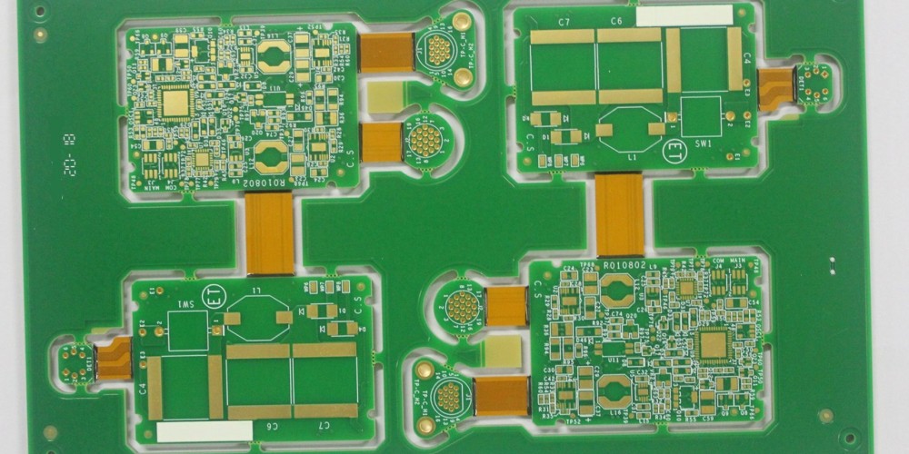
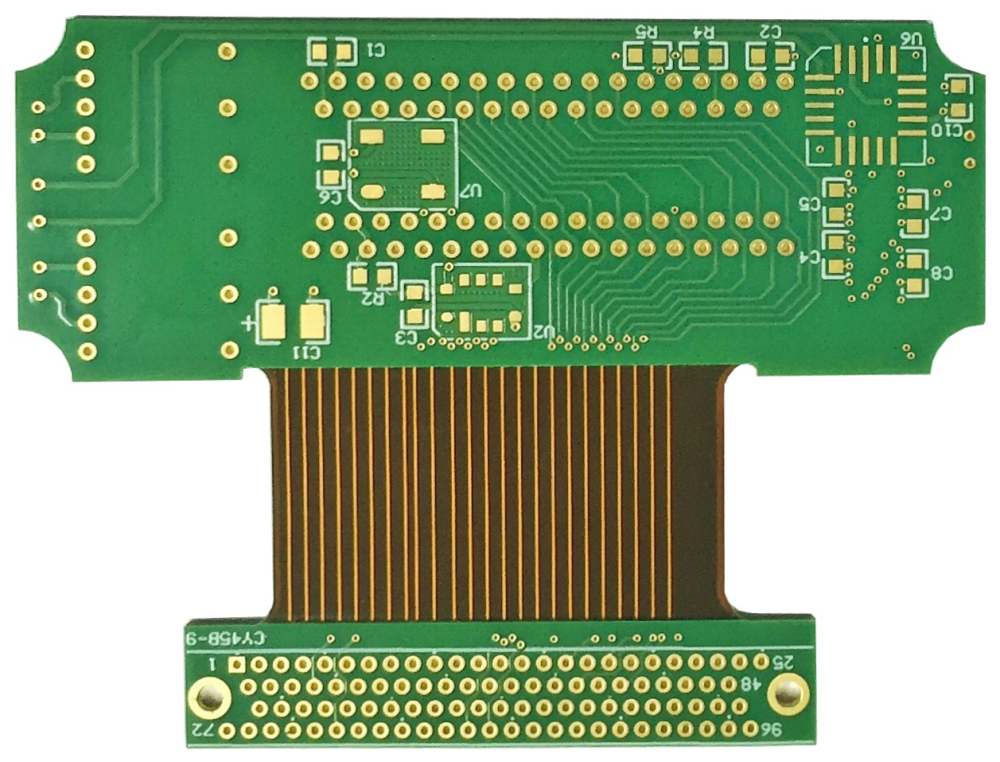
Rigid-flexible printed circuit boards (PCBs), also known as rigid flex circuits, are printed wiring boards that contain both rigid and flexible substrates laminated together. They provide solutions for complex electronics that require high density and space savings, as well as the ability to flex and fold into unique form factors.
8 layer rigid flex PCBs contain 8 conductive copper layers separated by dielectric materials. They offer advantages over fewer layer designs, including better signal integrity, increased routing channels, reduced EMI and crosstalk, and better power delivery. However, 8 layer rigid flex circuits are also more complex and expensive to design and manufacture.
This guide will provide a complete overview of 8 layer rigid flexible PCB technology, covering topics like:
- Benefits and applications
- Structure and materials
- Design considerations
- Manufacturing processes
- Quality control and testing
- Costs
Properly leveraging 8 layer rigid flex PCBs allows for innovative and reliable electronic products and systems across consumer, industrial, automotive, aerospace, medical, and military applications.
Benefits and Applications of 8 Layer Rigid Flex PCBs
There are several key benefits that 8 layer rigid flex PCBs provide:
- Higher routing density: The 8 copper layers allow for greater amounts of traces and components to be packed into a small space. This enables miniaturization and weight/space savings.
- Signal integrity: With more routing layers, signals can be isolated from each other to prevent crosstalk and EMI. Controlled impedance traces further improve signal performance.
- Lower impedance: 8 layers reduce the loop area between power and ground planes. This decreases impedance and improves power delivery to components.
- Flexibility: Rigid sections provide structural support while flexible sections allow bends, folds, and dynamic flexing. This enables unique form factors.
- Reliability: Rigid flex PCBs are extremely durable and resistant to shock, vibration, and flexing stresses. They have excellent thermal management as well.
Some common applications that leverage 8 layer rigid flex PCB technology include:
- Wearable electronics
- Internet of Things (IoT) devices
- Robotics and drones
- Automotive electronics
- Aerospace avionics
- Medical devices and equipment
- Military systems
- Consumer electronics
The combination of small size, excellent electrical performance, mechanical flexibility, and rugged reliability makes 8 layer rigid flex circuits ideal for advanced portable and compact electronics. The extra routing layers provide the density and signal quality needed in these applications.
Structure and Materials of 8 Layer Rigid Flex
8 layer rigid flex PCBs contain two key elements – rigid boards and flexible circuits – that are laminated together into one integrated assembly. Here are the typical material layers in an 8 layer stackup:
Rigid Layers
- Copper layers (1-8)
- FR-4 dielectric layers
- Prepreg bonding films
Flexible Layers
- Polyimide dielectric film
- Adhesive layers
Outer Layers
- Solder mask layer
- Silkscreen layer
The rigid sections of an 8 layer rigid flex PCB are made up of FR-4 material with woven glass reinforcement. This provides structural stability similar to a traditional PCB. FR-4 has good physical, electrical, and thermal properties.
The flexible sections use polyimide films such as Kapton. Polyimide has high tensile strength, excellent chemical resistance, and withstands repeated bending. It has a high glass transition temperature as well.
The rigid and flex materials are bonded together with adhesive prepreg films. These are usually thermosetting materials that get laminated under heat and pressure. The bond between sections manages stresses and prevents delamination.
On the outer surfaces, solder mask provides electrical insulation and environmental protection. Silkscreen prints identify components, connections, and board metrics.
Design Considerations for 8 Layer Rigid Flex
Designing an 8 layer rigid flex PCB requires attention to electrical, mechanical, and manufacturability requirements. Some key design guidelines include:
Layer Stackup
- Use symmetric stackups whenever possible, with evenly split ground/power/signal layers. This prevents warping.
- Mind the differences in copper thickness between inner and outer layers. Account for different etching rates.
- Place critical signals on inner layers for shielding when needed. High speed traces go on outer layers.
Trace Routing
- Use broader traces and spacing in the flex area since flex materials are less thermally conductive.
- Avoid acute angle trace turns in rigid-flex transition areas. Use teardrops and rounded corners.
- Leave enough clearance around drilled holes for pad shift during lamination.
Rigid-Flex Transition
- Distribute transition lines uniformly to reduce points of stress concentration.
- Do not place plated through-hole vias right at rigid-flex boundaries. Leave a safe margin.
- Use hatched copper or cross-hatched ground fills for better adhesion at transitions.
Component Placement
- Strategically place components to balance weight distribution across the rigid flex PCB.
- Group high power components together on the rigid section for heat sinking.
- Watch component spacing at rigid-flex bends to prevent collisions during flexing.
Flex Areas
- Minimize unsupported spans in dynamic flex areas to avoid metal fatigue over time.
- Design controlled impedance flex traces for high frequency signals like PCIe or USB 3.0.
- Allow space for stiffeners, shields, or support structures in the flex area if needed.
Proper 8 layer rigid flex design is critical to ensuring the PCB’s electrical performance, mechanical robustness, and manufacturing yield.
Manufacturing Processes for 8 Layer Rigid Flex
Producing reliable and high-quality 8 layer rigid flex PCBs requires specialized fabrication techniques and workflows. Here is an overview of key manufacturing processes:
Lamination
- Align all material layers and use precision lamination presses to bond under heat and pressure.
- Laminate rigid and flex sections separately first before doing the final overall lamination.
- Use locally controllable vacuum laminators to apply specific pressures across a board.
Drilling
- Use optimized twist drills for rigid sections and special diamond-coated drills for flex areas.
- Employ depth control equipment like laser hole detectors to handle different drill rates.
- Plunge drill holes at rigid-flex transitions to avoid tear outs.
Metallization
- Deposit conformal copper in blind and buried vias and microvias with sputter coating or electroless plating.
- Electrolytically plate copper to required trace thicknesses across rigid and flex areas.
- Use different plating profiles for inner and outer layers based on dielectric material.
Etching
- Utilize print-and-etch processes to define fine trace geometries.
- Etch rigid and flexible sections separately using cupric chloride and ammoniacal etchants tailored for each material.
Solder Mask and Silkscreen
- Apply solder mask in two coats using liquid photoimageable or dry film coatings.
- Use flex-grade mask to withstand flexing stresses.
- Print component overlays and board information with durable epoxy ink.
Final Testing
- Test for opens, shorts, impedance, signal speed, continuity before boards leave the factory.
- Perform rigorous mechanical flexure testing on finished boards.
- Conduct thermal stress tests for mission-critical applications.
8 layer rigid flex PCB fabrication requires specialized materials, equipment, and processes to produce high-reliability printed wiring boards.
Quality Control and Testing
Verifying the quality and reliability of finished 8 layer rigid flex PCBs is critical before they are deployed in end products. Some key testing and inspection methods include:
Electrical Testing
- Flying probe testing checks for electrical opens, shorts, and impedance.
- ICT fixtures verify nets and component connections on loaded boards.
- Signal integrity analysis using TDR/TDT measures losses and propagation delay.
Test Points
- Include test points connected to internal layers for probing during debug.
- Allow test access to critical nets and buses for boundary scans.
Automated Optical Inspection
- AOI systems check trace spacing, pad registration, solder mask dams.
- 3D AOI verifies plated through hole integrity.
- Confirms proper layer-to-layer alignment.
X-Ray Inspection
- X-ray laminography detects potential buried defects like voids.
- Images internal layer continuity and misalignments.
- Useful for inspecting BGAs and other hidden solder joints.
Mechanical Testing
- Flexural endurance testing qualifies dynamic bending performance.
- Vibration testing verifies robustness to real-world G-forces.
- Thermal cycling confirms material integrity over temperature shifts.
Cross-Sectioning
- Cross-sectioned micrographs reveal layer registration and bond line quality.
- Allows detailed inspection of plated through holes and microvias.
Rigorous testing and inspection ensures 8 layer rigid flex PCBs meet all electrical, mechanical, and manufacturing requirements before deployment.
Cost Factors for 8 Layer Rigid Flex Circuits
Some of the key factors that contribute to cost of 8 layer rigid flexible PCBs:
- Number of layers – Each additional conductive layer adds expense for materials, processing, and thickness. 8 layers is costlier than 6 or 4 layer.
- Board size – Larger boards require more raw materials and take longer to fabricate, increasing cost.
- Design complexity – Dense routing, HDI technologies, and challenging layouts require more engineering effort.
- Flex vs rigid ratio – More flex area means costlier flexible dielectric materials. High rigid ratio lowers cost.
- Volume – Higher order volumes achieve economies of scale and allow price breaks per board.
- Special processes – Advanced steps like blind/buried vias, flex patterning add cost.
- Testing and certification – Rigorous qualification, inspection, and documentation increases cost.
- Lead time – Faster fabrication turnarounds increase costs due to additional shifts and expedited processing.
- Location – Local US or European production is more expensive than Asian sourcing.
In general, 8 layer rigid flex PCBs range from $800 to $3000 depending on size, volume, and complexity. The benefits of increased routing density, signal integrity, and flexibility outweigh the higher costs for many applications.
Frequently Asked Questions
Q: What are some differences between 6 layer and 8 layer rigid flex PCBs?
A: 8 layer designs offer two extra routing layers for increased density and isolation. They also provide lower impedance and better power distribution with the additional reference planes. The cost is higher, but 8 layers future-proofs designs better as complexity increases.
Q: Can 8 layer rigid flex PCBs incorporate embedded passives and components?
A: Yes, technologies like laser direct structuring (LDS) allow passive components like resistors and capacitors to be embedded into the PCB itself. This helps save space and cost compared to discrete surface mount components. LDS works well with 8 layer rigid-flex.
Q: How small can the bend radius be for flexible sections of rigid flex PCBs?
A: The bend radius depends on the thickness of the polyimide material used. Typical bend radii range from 3 to 10 times the total board thickness. Dynamic flex areas need larger radii than static bends to avoid metal fatigue over lifetime motion.
Q: What are some best practices for transitioning signals between rigid and flex sections?
A: Use ground vias next to signal vias at transitions to reduce impedance discontinuities. Route critical signals on inner layers first, then less critical signals on outer layers. Avoid routing high speed traces across bends. Use cross-hatched copper fills for stability.
Q: What types of connectors work well for 8 layer rigid flex PCBs?
A: High density connectors like those with 0.4mm pitch allow maximizing input/output connections. Flex-tail connectors accommodate dynamic motion across bends. Board-to-board connectors work for stacking or interconnection. Micro coax, pogo pins also work well.
In summary, 8 layer rigid flexible PCBs provide an invaluable technology solution for advanced electronics and systems that require miniaturization, performance, and reliability. Careful design and fabrication is needed to leverage their benefits fully. This guide covers key considerations across the entire 8 layer rigid flex PCB development and production cycle.