


Introduction to 4 Layer Rigid Flex PCBs
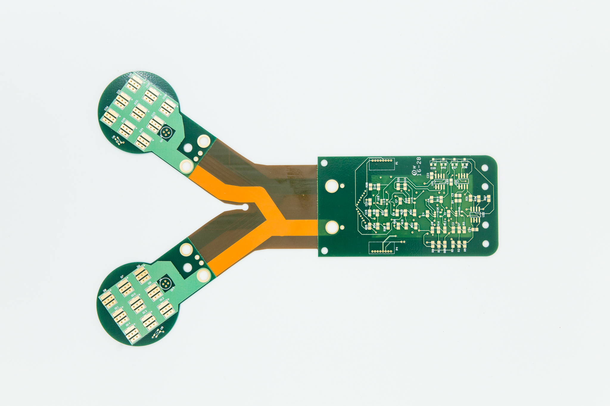
A rigid-flex PCB is a printed circuit board that contains both rigid and flexible substrates laminated together to provide mechanical support as well as flexibility. The rigid sections provide stability while the flexible sections allow for dynamic configurations and three-dimensional placements.
A 4 layer rigid-flex PCB contains 4 conductive layers with copper traces for routing signals and power. Two internal layers are sandwiched between two external layers. The cross-section of a 4 layer rigid-flex PCB would show 4 copper layers separated by dielectric material.
Some key benefits of 4 layer rigid-flex PCBs:
- More routing channels for high density interconnections
- Good EMI shielding when ground planes are incorporated
- Allows for impedance control compared to 2 layer boards
- Handles higher current levels due to thicker copper
Some applications where 4 layer rigid-flex PCBs are used:
- Consumer electronics – Cell phones, laptops, VR devices
- Automotive – Advanced Driver Assistance Systems (ADAS)
- Medical – Imaging systems, hearing aids
- Industrial – Robotics, instrumentation
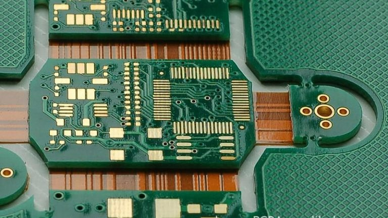
Rigid vs Flexible Sections
The rigid sections of the PCB provide structural stability for mounting components while the flexible sections allow dynamic movements and three-dimensional configuration.
For the rigid sections, standard PCB materials like FR-4 or high frequency substrates are used. The flexible sections use polyimide or other flexible polymer materials.
During layout, components are generally placed on the rigid sections while interconnections between sections are routed through the flexible layers. The rigid sections can have 4 or more layers while flexible sections are typically 2 layers.
Determining Rigid vs Flex Areas
Here are some guidelines for determining rigid and flexible sections:
- Place components on rigid sections for stability
- Minimize components on flexible areas
- High speed traces should be routed on rigid sections
- Avoid 90 degree or sharp bends in flexible sections
- Keep flexible sections short, around 25-100mm ideal
- Ensure proper coverage of soldermask over flexible areas
Stackup Design
The stackup refers to the sequence of dielectric, copper foil, and coverlay materials used in the PCB. A well designed stackup is critical for routing, impedance control, and manufacturability.
Here are some key considerations for 4 layer rigid-flex stackups:
- Dielectric materials – Use FR-4 or high frequency material for rigid sections. Use polyimide for flexible sections. Match Dk values.
- Copper thickness – 1oz (35um) commonly used. Can increase to 2oz for higher current capacity
- Layer sequence – Ensure adjacent layers are routed in orthogonal directions to avoid crosstalk
- Impedance – Maintain consistent dielectric thicknesses between signal layers
- Flex layer placement – Place ground layers adjacent to flexible sections for shielding
A sample 4 layer rigid-flex stackup:
This provides good isolation between signals while maintaining consistent impedance.
Layout and Routing
Rigid-flex PCB layout follows similar principles as rigid PCBs, but requires special considerations at the rigid-flex interfaces. Here are some key guidelines:
- Minimize components in flex area
- Avoid routing high speed signals through flex
- Use teardrop pads for traces entering rigid sections
- Include strain relief patterns at rigid-flex junctions
- Maintain minimum bend radius in flex areas
- Verify impedance consistency through rigid and flex sections
In addition, safe distances must be maintained between conductors in the flexing areas. Use larger spacing and tighter tolerances for flexible layer fabrication.
Materials and Manufacturing
Rigid-flex PCB fabrication requires specialized materials and processes:
- Masking – Areas are masked using photoresist or rubber dams during lamination
- Layup – Rigid and flex materials are precisely laminated together
- Registration – Excellent layer-to-layer registration is critical
- Etching – Etching must be done after lamination
- Coverlay – Polyimide coverlay is added for protection of flexible layers
- Soldermask – LPI soldermask is typically used for protection in flexing areas
- Via Construction – Plated through hole vias, buried vias and microvias used
- Testing – Both electrical testing and bend cycle testing performed
Work with a manufacturer experienced in rigid-flex PCB fabrication to ensure quality and reliability.
Applications of 4 Layer Rigid Flex Circuits
Here are some common applications taking advantage of 4 layer rigid-flex PCB technology:
Consumer Electronics
- Cell phones – Allow compact folding and protect flexing interconnections
- Laptops – Interconnect motherboard and display while allowing hinge movement
- Wearables – Facilitate flexible wristbands and wearable sensor devices
- VR/AR – Headset goggles with flexing interconnects to electronics
Automotive
- Advanced driver assistance systems – Sensor integration in tight spaces
- Infotainment – Dynamic center console and touchscreen designs
- Lighting systems – Integration of headlights and taillights
Medical
- Hearing aids – Flexible circuits for compact fit in ear
- Imaging systems – Circuits to control detectors and sensors
- Implants – Flexible interconnects for implants and wearable devices
Industrial
- Robotics – Pretztail cable replacement for moving joints
- Instrumentation – Compact interconnects for handheld devices
- Avionics – Circuits for aerospace applications
Pros and Cons of 4 Layer Rigid Flex
Pros
- Increased routing density compared to 2 layer flex
- Good for impedance control and high speed signals
- Thicker copper layers handle higher current levels
- Stiffener layers provide good mechanical support
- Effective EMI shielding when ground layers are used
- Enables 3D circuit configurations
- Dynamic movements and flexing possible
- More miniaturization in product designs
Cons
- More complex fabrication process
- Requires specialized design expertise
- Motion limitations to avoid flex damage
- Generally more expensive than rigid PCBs
- Design and assembly challenges at rigid-flex junction
- Requires excellent rigid-flex registration
Frequently Asked Questions
Here are some common questions about 4 layer rigid flex PCB design and manufacturing:
What are the typical dielectric materials used?
For rigid sections, FR-4 and high frequency materials like Megtron 6 are commonly used. Flexible sections use polyimide films like Kapton or UPILEX. adhesive layers bond the materials.
What are recommended trace widths and spacing?
Follow IPC 2221 standards. Typical trace/space is 6/6 mil (0.15mm) in rigid sections. Use 8/8 mil (0.2mm) or more in flex areas.
What bend radius should be maintained in flex areas?
Minimum bend radius should be at least 10 times the total flex thickness. Typical flex thickness is ~3-5mil so 30-50mil radius is recommended.
How many rigid layers are typical for a rigid-flex PCB?
2 to 8+ rigid layers can be used if needed, but 4 metal layers is typical for many applications to balance cost, routing density and stiffness.
What types of vias are used in rigid-flex PCBs?
Plated through hole vias in rigid sections. Microvias or buried vias can connect outer layers through inner layers. Blind or buried vias connect flex layers.
How are components attached in rigid vs. flex areas?
SMT components are attached in rigid sections. Avoid placing components in flex areas if possible. Use glue or encapsulation if needed.
How is impedance controlled between rigid and flex sections?
Maintain same dielectric materials and thicknesses between signal reference planes through both sections. Adjust trace widths to tune impedance.
What testing should be done to verify a rigid-flex design?
Electrical testing checks continuity, shorts and function. Dynamic bend cycle testing flexes the board thousands of times to check reliability.