


Understanding the Basics of Microwave PCB Design
Before diving into the design process, it’s crucial to understand the fundamentals of microwave PCBs and how they differ from traditional PCBs.
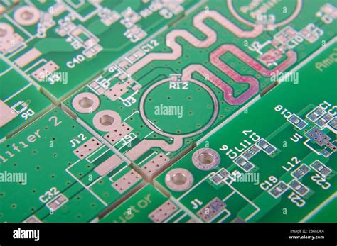
What is a Microwave PCB?
A microwave PCB is a printed circuit board specifically designed to handle high-frequency signals, typically in the range of 300 MHz to 300 GHz. These PCBs are used in various applications, such as wireless communications, radar systems, and satellite technology.
Key Considerations for Microwave PCB Design
When designing microwave PCBs, several key factors must be taken into account:
- Material selection
- Impedance matching
- Signal integrity
- Thermal management
- Manufacturability
Step 1: Define Your Microwave PCB Requirements
The first step in designing a microwave PCB is to clearly define your requirements. This includes:
- Frequency range
- Power handling capabilities
- Signal integrity
- Physical dimensions
- Environmental conditions
By establishing these requirements early on, you can ensure that your design meets the necessary specifications and constraints.

Step 2: Choose the Right Substrate Material
Selecting the appropriate substrate material is crucial for microwave PCB performance. Some common substrate materials include:
- Rogers RO4000 series
- Isola I-Tera MT40
- Taconic RF-35
- PTFE (Polytetrafluoroethylene)
Consider factors such as dielectric constant, dissipation factor, and thermal stability when choosing your substrate material.

Step 3: Determine the Layer Stack-up
The layer stack-up of your microwave PCB plays a significant role in signal integrity and impedance matching. A typical microwave PCB layer stack-up may include:
- Top layer (signal)
- Ground plane
- Dielectric layer
- Power plane
- Bottom layer (signal)
Ensure that your layer stack-up is optimized for your specific application and frequency range.

Step 4: Design the Microstrip or Stripline Traces
Microstrip and stripline traces are the most common transmission line structures used in microwave PCBs. When designing these traces, consider the following:
- Trace width and thickness
- Characteristic impedance
- Losses and dispersion
- Coupling and crosstalk
Use appropriate equations and simulation tools to optimize your trace design for optimal signal integrity.
Step 5: Implement Impedance Matching Techniques
Impedance matching is essential for minimizing signal reflections and ensuring maximum power transfer. Some common impedance matching techniques include:
- Quarter-wave transformers
- Tapered lines
- Stub matching
- Resistive matching
Choose the most suitable technique based on your specific application and design constraints.
Step 6: Design Passive Components
Passive components, such as filters, couplers, and power dividers, are crucial elements in microwave PCB design. When designing these components, consider:
- Frequency response
- Insertion loss
- Return loss
- Bandwidth
- Physical size
Use appropriate design tools and simulation software to optimize your passive component designs.
Step 7: Place and Route Components
Proper placement and routing of components on your microwave PCB are essential for minimizing signal interference and ensuring optimal performance. Consider the following:
- Component orientation
- Trace routing
- Grounding and shielding
- Thermal management
Use CAD tools and design rules to ensure proper placement and routing of your components.
Step 8: Simulate and Optimize Your Design
Before fabricating your microwave PCB, it’s essential to simulate and optimize your design using appropriate software tools. This includes:
- Electromagnetic (EM) simulation
- Circuit simulation
- Thermal simulation
- Signal integrity analysis
Iteratively refine your design based on simulation results to achieve the best possible performance.
Step 9: Design for Manufacturability (DFM)
Designing for manufacturability is crucial to ensure that your microwave PCB can be produced efficiently and reliably. Consider the following DFM guidelines:
- Minimum trace width and spacing
- Via size and placement
- Soldermask and silkscreen
- Panelization and breakaway tabs
Work closely with your PCB manufacturer to ensure that your design meets their specific DFM requirements.
Step 10: Generate Manufacturing Files
Once your design is finalized, generate the necessary manufacturing files for your PCB fabricator. These files typically include:
- Gerber files
- Drill files
- BOM (Bill of Materials)
- Fabrication drawings
Ensure that your manufacturing files are accurate and complete to avoid delays and potential issues during production.
Step 11: Fabricate Prototypes
Before mass production, it’s essential to fabricate prototypes of your microwave PCB for testing and validation. Work with a reputable PCB manufacturer that has experience in producing high-frequency PCBs.
Step 12: Assemble Components
After receiving your fabricated PCB Prototypes, assemble the components using appropriate soldering techniques. For microwave PCBs, consider using:
- Reflow soldering
- Hand soldering (for larger components)
- Automated pick-and-place (for surface-mount components)
Ensure that your assembly process follows proper ESD (Electrostatic Discharge) precautions to prevent damage to sensitive components.
Step 13: Test and Validate Your Design
Once your microwave PCB Prototypes are assembled, it’s time to test and validate your design. This may include:
- S-parameter measurements
- Power handling tests
- Thermal tests
- EMC (Electromagnetic Compatibility) tests
Compare your test results with your initial design requirements and make any necessary adjustments to optimize performance.
Step 14: Refine and Iterate
Based on the results of your testing and validation, refine and iterate your microwave PCB design as needed. This may involve:
- Adjusting component values
- Modifying trace geometries
- Improving grounding and shielding
- Optimizing thermal management
Repeat the simulation, fabrication, assembly, and testing steps until your design meets all performance and reliability requirements.
Step 15: Prepare for Mass Production
Once your microwave PCB design is finalized and validated, prepare for mass production. This includes:
- Finalizing manufacturing files
- Selecting a PCB fabricator and assembly partner
- Establishing quality control procedures
- Planning for logistics and inventory management
Work closely with your manufacturing partners to ensure a smooth transition to mass production.
Step 16: Monitor and Improve
Even after your microwave PCB is in mass production, it’s essential to continuously monitor and improve your design. This may involve:
- Collecting field data and customer feedback
- Analyzing failure modes and implementing corrective actions
- Exploring new materials and technologies
- Optimizing your manufacturing process
By continuously monitoring and improving your microwave PCB design, you can ensure long-term success and customer satisfaction.
Frequently Asked Questions (FAQ)
1. What is the difference between a microwave PCB and a regular PCB?
A microwave PCB is designed to handle high-frequency signals (typically 300 MHz to 300 GHz), while a regular PCB operates at lower frequencies. Microwave PCBs require specialized materials, design techniques, and manufacturing processes to ensure optimal performance and signal integrity.
2. What are some common applications for microwave PCBs?
Microwave PCBs are used in various applications, including:
- Wireless communications (5G, Wi-Fi, Bluetooth)
- Radar systems
- Satellite technology
- Aerospace and defense
- Medical devices
3. What is the importance of impedance matching in microwave PCB design?
Impedance matching is crucial in microwave PCB design to minimize signal reflections and ensure maximum power transfer. Mismatched impedances can lead to signal degradation, reduced efficiency, and potential damage to components.
4. How do I choose the right substrate material for my microwave PCB?
When selecting a substrate material for your microwave PCB, consider factors such as:
- Dielectric constant
- Dissipation factor
- Thermal stability
- Cost
- Availability
Some common substrate materials for microwave PCBs include Rogers RO4000 series, Isola I-Tera MT40, Taconic RF-35, and PTFE.
5. What are some best practices for designing for manufacturability (DFM) in microwave PCBs?
To ensure that your microwave PCB can be manufactured efficiently and reliably, follow these DFM best practices:
- Adhere to minimum trace width and spacing requirements
- Use appropriate via sizes and placement
- Ensure proper soldermask and silkscreen coverage
- Implement panelization and breakaway tabs for easy separation
- Work closely with your PCB manufacturer to understand their specific DFM guidelines
By understanding and following these 16 steps, you can successfully design, manufacture, and optimize microwave PCBs for a wide range of applications. Remember to continuously monitor and improve your design to ensure long-term success and customer satisfaction.